


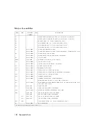

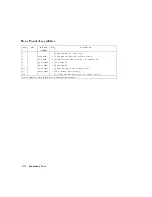


A4/A5/A6
Sampler/Mixer
The
A4,
A5,
and
A6
sampler/mixers
all
down-convert
the
RF
input
signals
to
xed
4
kHz
2nd
IF
signals
with
amplitude
and
phase
corresponding
to
the
RF
input.
F
or
the
analyzer
with
with
Option
006,
the
A6
B
sampler/mixer
assembly
includes
an
8
dB
gain
preamplier
in
front
of
the
sampler
.
This
improves
the
noise
gure
performance
of
the
analyzer's
receiver
channel
B
.
The
Sampler
Circuit
in
High
Band
In
high
band
operation,
the
sampling
rate
of
the
samplers
is
controlled
by
the
1st
LO
from
the
A7
pulse
generator
assembly
.
The
1st
LO
is
a
comb
of
harmonics
produced
by
a
step
recovery
diode
driven
by
the
fractional-N
V
CO
fundamental
signal.
One
of
the
harmonic
signals
is
1
MHz
below
the
start
frequency
set
at
the
front
panel.
The
1st
LO
is
combined
in
the
samplers
with
the
source
output
signal.
In
options
003
and
006,
samplers
are
additionally
capable
of
receiving
RF
input
signals
up
to
3
and
6
GHz
respectively
.
The
mixing
products
are
ltered,
so
that
the
only
remaining
response
is
the
dierence
between
the
source
frequency
and
the
harmonic
1
MHz
below
it.
This
xed
1
MHz
signal
is
the
1st
IF
.
P
art
of
the
1st
IF
signal
from
the
A4
R
sampler
is
fed
back
to
the
A11
phase
lock
assembly
.
The
Sampler
Circuit
in
Low
Band
In
low
band
the
sampler
diodes
are
biased
continuously
on,
so
that
the
RF
input
signal
passes
through
them
unchanged.
Thus
the
1st
IF
is
identical
to
the
RF
output
signal
from
the
source
(300
kHz
to
16
MHz),
and
sweeps
with
it.
P
art
of
the
1st
IF
signal
from
the
A4
R
sampler
is
fed
back
to
the
A11
phase
lock
assembly
.
(Refer
to
\Source
Theory
Overview"
for
information
on
high
band
and
low
band
operation
of
the
source
.)
The
2nd
LO
Signal
The
2nd
LO
is
obtained
from
the
A12
reference
assembly
.
In
high
band,
the
2nd
LO
is
xed
at
996
kHz.
This
is
produced
by
feeding
the
39.84
MHz
output
of
a
phase-locked
oscillator
in
the
A12
assembly
through
a
divide-by-40
circuit.
In
low
band,
the
2nd
LO
is
a
variable
frequency
produced
by
mixing
the
output
of
the
fractional-N
V
CO
with
a
xed
39.996
MHz
signal
in
the
A12
assembly
.
The
2nd
LO
covers
the
range
of
0.014
to
16.004
MHz
in
two
subsweeps
that
correspond
with
the
source
subsweeps
.
These
subsweeps
are
0.304
to
3.304
MHz
and
3.304
to
16.004
MHz.
12-28
Theory
of
Operation
Содержание 8752C
Страница 22: ...Before Applying Power 15 6 Servicing 15 6 Index Contents 16 ...
Страница 38: ......
Страница 43: ...Figure 2 1 Measurement Uncertainty Window System Veri cation and Performance Tests 2 5 ...
Страница 80: ...Figure 2 15 Magnitude Dynamic Accuracy Test Setup 2 42 System Veri cation and Performance Tests ...
Страница 116: ......
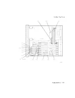
Страница 122: ...Figure 3 1 Location of Major Assemblies 3 6 Adjustments and Correction Constants ...
Страница 176: ......
Страница 192: ...4 16 Start Troubleshooting Here ...
Страница 193: ......
Страница 194: ...Figure 4 7 HP 8752C Overall Block Diagram 2 of 4 Option 003 and 004 Start Troubleshooting Here 4 19 ...
Страница 195: ...Figure 4 7 HP 8752C Overall Block Diagram 3 of 4 Option 006 4 20 Start Troubleshooting Here ...
Страница 196: ...Figure 4 7 HP 8752C Overall Block Diagram 4 of 4 Option 004 and 006 Start Troubleshooting Here 4 21 ...
Страница 197: ......
Страница 221: ...5 24 Power Supply Troubleshooting ...
Страница 222: ......
Страница 225: ...Digital Control Group Block Diagram Figure 6 1 Digital Control Group Block Diagram Digital Control Troubleshooting 6 3 ...
Страница 267: ...Figure 7 18 25 MHz HI OUT Waveform from A14J1 Figure 7 19 60 MHz HI OUT Waveform from A14J1 Source Troubleshooting 7 27 ...
Страница 271: ...Figure 7 21 A14 Generated Digital Control Signals Source Troubleshooting 7 31 ...
Страница 301: ...Figure 9 2 Typical Smith Chart Traces of Good Short a and Open b Accessories Troubleshooting 9 7 ...
Страница 302: ......
Страница 366: ......
Страница 378: ...Figure 11 4 Typical ED Re ection Test Port 11 12 Error Terms ...
Страница 380: ...Figure 11 5 Typical ES Re ection Test Port 11 14 Error Terms ...
Страница 382: ...Figure 11 6 Typical ER Re ection Test Port 11 16 Error Terms ...
Страница 384: ...Figure 11 7 Typical EX with 10 Hz Bandwidth Figure 11 8 Typical EX with 3 kHz Bandwidth 11 18 Error Terms ...
Страница 386: ...Figure 11 9 Typical ET 11 20 Error Terms ...
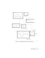
Страница 407: ...Figure 12 5 High Band Operation of the Source Theory of Operation 12 21 ...
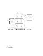
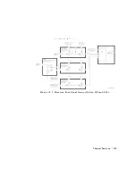
Страница 410: ...Figure 12 6 Receiver Functional Group standard and Option 003 12 24 Theory of Operation ...
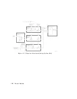
Страница 411: ...Figure 12 7 Receiver Functional Group Option 003 and 004 Theory of Operation 12 25 ...
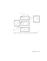
Страница 412: ...Figure 12 8 Receiver Functional Group Option 006 12 26 Theory of Operation ...
Страница 413: ...Figure 12 9 Receiver Functional Group Option 004 and 006 Theory of Operation 12 27 ...
Страница 416: ......
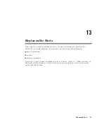
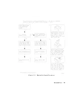
Страница 419: ...Figure 13 1 Module Exchange Procedure Replaceable Parts 13 3 ...
Страница 423: ...Major Assemblies Replaceable Parts 13 7 ...
Страница 425: ...Front Panel Assemblies Replaceable Parts 13 9 ...
Страница 427: ...Rear Panel Assemblies Replaceable Parts 13 11 ...
Страница 429: ...Cables Top View Replaceable Parts 13 13 ...
Страница 431: ...Front Panel Cables and Attaching Hardware Replaceable Parts 13 15 ...
Страница 433: ...Rear Panel Cables and Attaching Hardware Replaceable Parts 13 17 ...
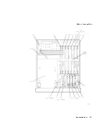
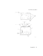
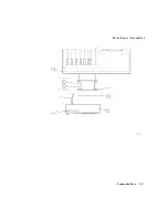
Страница 435: ...Source and Sampler Parts Standard and Option 003 Replaceable Parts 13 19 ...
Страница 437: ...Source and Sampler Parts Option 004 006 Replaceable Parts 13 21 ...
Страница 439: ...Source and Sampler Parts Options 004 and 003 004 Replaceable Parts 13 23 ...
Страница 441: ...Source and Sampler Parts Option 006 Replaceable Parts 13 25 ...
Страница 443: ...Display Bezel Assembly Replaceable Parts 13 27 ...
Страница 445: ...Chassis Parts Replaceable Parts 13 29 ...
Страница 447: ...Top View of Attaching Hardware and Post Regulator Fuses Replaceable Parts 13 31 ...
Страница 449: ...Bottom View of Attaching Hardware Replaceable Parts 13 33 ...
Страница 488: ......