
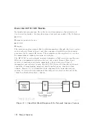


A2
Front
P
anel
Processor
The
A2
front
panel
processor
detects
and
decodes
user
inputs
from
the
front
panel
keys
and
RPG
knob
,
and
transmits
them
to
the
CPU
.
It
has
the
capability
to
interrupt
the
CPU
to
provide
information
updates
.
It
also
controls
the
front
panel
LEDs
that
provide
status
information
to
the
user
.
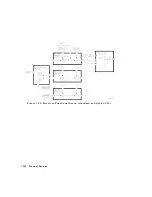
A9
CPU/A10
Digital
IF
The
A9
CPU
assembly
contains
the
main
CPU
(central
processing
unit),
the
digital
signal
processor
,
memory
storage
.
The
main
CPU
is
the
master
controller
for
the
analyzer
,
including
the
other
dedicated
microprocessors
.
The
memory
includes
EEPROM,
RAM,
EPROM,
and
ROM.
Data
from
the
receiver
is
serially
clocked
into
the
A9
CPU
assembly
from
the
A10
digital
IF
.
The
data-taking
sequence
is
triggered
either
from
the
A14
fractional-N
assembly
,
externally
from
the
rear
panel,
or
by
rmware
on
the
A9
assembly
.
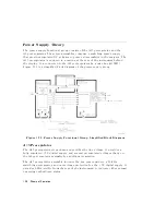
Main
CPU
The
main
CPU
is
a
16-bit
microprocessor
that
maintains
digital
control
over
the
entire
instrument
through
the
instrument
bus
.
The
main
CPU
receives
external
control
information
from
the
front
panel
or
HP-IB
,
and
performs
processing
and
formatting
operations
on
the
raw
data
in
the
main
RAM.
It
controls
the
digital
signal
processor
,
the
front
panel
processor
,
the
display
processor
,
and
the
interconnect
port
interfaces
.
In
addition,
when
the
analyzer
is
in
the
system
controller
mode
,
the
main
CPU
controls
peripheral
devices
through
the
peripheral
port
interfaces
.
The
main
CPU
has
a
dedicated
EPROM
that
contains
the
operating
system
for
instrument
control.
Front
panel
settings
are
stored
in
CMOS
RAM,
with
a
battery
providing
at
least
5
years
of
backup
storage
when
external
power
is
switched
o.
Main
RAM
The
main
RAM
(random
access
memory)
is
shared
memory
for
the
CPU
and
the
digital
signal
processor
.
It
stores
the
raw
data
received
from
the
digital
signal
processor
,
while
additional
calculations
are
performed
on
it
by
the
CPU
.
The
CPU
reads
the
resulting
formatted
data
from
the
main
RAM
and
converts
it
to
GSP
commands
.
It
writes
these
commands
to
the
GSP
for
output
to
the
analyzer's
display
.
Theory
of
Operation
12-11
Содержание 8752C
Страница 22: ...Before Applying Power 15 6 Servicing 15 6 Index Contents 16 ...
Страница 38: ......
Страница 43: ...Figure 2 1 Measurement Uncertainty Window System Veri cation and Performance Tests 2 5 ...
Страница 80: ...Figure 2 15 Magnitude Dynamic Accuracy Test Setup 2 42 System Veri cation and Performance Tests ...
Страница 116: ......
Страница 122: ...Figure 3 1 Location of Major Assemblies 3 6 Adjustments and Correction Constants ...
Страница 176: ......
Страница 192: ...4 16 Start Troubleshooting Here ...
Страница 193: ......
Страница 194: ...Figure 4 7 HP 8752C Overall Block Diagram 2 of 4 Option 003 and 004 Start Troubleshooting Here 4 19 ...
Страница 195: ...Figure 4 7 HP 8752C Overall Block Diagram 3 of 4 Option 006 4 20 Start Troubleshooting Here ...
Страница 196: ...Figure 4 7 HP 8752C Overall Block Diagram 4 of 4 Option 004 and 006 Start Troubleshooting Here 4 21 ...
Страница 197: ......
Страница 221: ...5 24 Power Supply Troubleshooting ...
Страница 222: ......
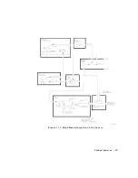
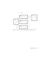
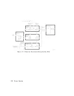
Страница 225: ...Digital Control Group Block Diagram Figure 6 1 Digital Control Group Block Diagram Digital Control Troubleshooting 6 3 ...
Страница 267: ...Figure 7 18 25 MHz HI OUT Waveform from A14J1 Figure 7 19 60 MHz HI OUT Waveform from A14J1 Source Troubleshooting 7 27 ...
Страница 271: ...Figure 7 21 A14 Generated Digital Control Signals Source Troubleshooting 7 31 ...
Страница 301: ...Figure 9 2 Typical Smith Chart Traces of Good Short a and Open b Accessories Troubleshooting 9 7 ...
Страница 302: ......
Страница 366: ......
Страница 378: ...Figure 11 4 Typical ED Re ection Test Port 11 12 Error Terms ...
Страница 380: ...Figure 11 5 Typical ES Re ection Test Port 11 14 Error Terms ...
Страница 382: ...Figure 11 6 Typical ER Re ection Test Port 11 16 Error Terms ...
Страница 384: ...Figure 11 7 Typical EX with 10 Hz Bandwidth Figure 11 8 Typical EX with 3 kHz Bandwidth 11 18 Error Terms ...
Страница 386: ...Figure 11 9 Typical ET 11 20 Error Terms ...
Страница 407: ...Figure 12 5 High Band Operation of the Source Theory of Operation 12 21 ...
Страница 410: ...Figure 12 6 Receiver Functional Group standard and Option 003 12 24 Theory of Operation ...
Страница 411: ...Figure 12 7 Receiver Functional Group Option 003 and 004 Theory of Operation 12 25 ...
Страница 412: ...Figure 12 8 Receiver Functional Group Option 006 12 26 Theory of Operation ...
Страница 413: ...Figure 12 9 Receiver Functional Group Option 004 and 006 Theory of Operation 12 27 ...
Страница 416: ......
Страница 419: ...Figure 13 1 Module Exchange Procedure Replaceable Parts 13 3 ...
Страница 423: ...Major Assemblies Replaceable Parts 13 7 ...
Страница 425: ...Front Panel Assemblies Replaceable Parts 13 9 ...
Страница 427: ...Rear Panel Assemblies Replaceable Parts 13 11 ...
Страница 429: ...Cables Top View Replaceable Parts 13 13 ...
Страница 431: ...Front Panel Cables and Attaching Hardware Replaceable Parts 13 15 ...
Страница 433: ...Rear Panel Cables and Attaching Hardware Replaceable Parts 13 17 ...
Страница 435: ...Source and Sampler Parts Standard and Option 003 Replaceable Parts 13 19 ...
Страница 437: ...Source and Sampler Parts Option 004 006 Replaceable Parts 13 21 ...
Страница 439: ...Source and Sampler Parts Options 004 and 003 004 Replaceable Parts 13 23 ...
Страница 441: ...Source and Sampler Parts Option 006 Replaceable Parts 13 25 ...
Страница 443: ...Display Bezel Assembly Replaceable Parts 13 27 ...
Страница 445: ...Chassis Parts Replaceable Parts 13 29 ...
Страница 447: ...Top View of Attaching Hardware and Post Regulator Fuses Replaceable Parts 13 31 ...
Страница 449: ...Bottom View of Attaching Hardware Replaceable Parts 13 33 ...
Страница 488: ......