


EM358x
Rev. 0.4
227
± 20 mV. If better absolute accuracy is required, the ADC can be configured to use an external reference. The
ADC calibrates as a single-ended measurement. Differential signals require correction of both their inputs.
The following steps outline the calibration procedure
Calibrate VREF against VDD_PADSA.
Determine the ADC gain by sampling independently VREF and GND. Gain is calculated from the slope of
these two measurements.
Apply gain correction.
Determine the ADC offset by sampling GND.
Apply offset correction.
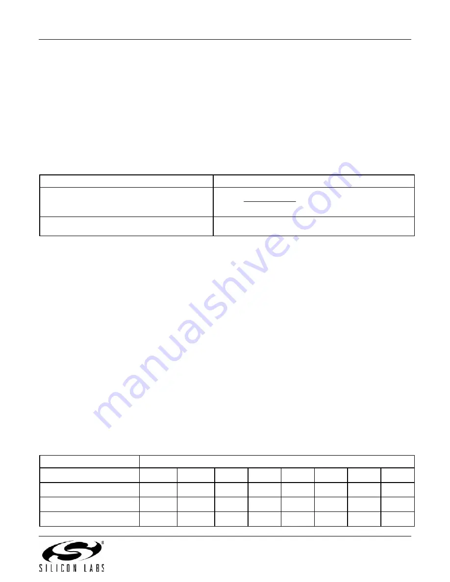
Table 11-5 shows the equations used to calculate the gain and offset correction values.
Table 11-5. ADC Gain and offset correction equations
Calibration
Correction value
Gain
)
(
16384
32768
GND
VREF
N
N
Offset ( after applying gain correction )
)
57344
(
2
GND
N
Equation notes
The ADC output is two’s complement. All N are therefore 16-bit two’s complement numbers.
Offset is a 16-bit two’s complement number.
Gain is a 16-bit number representing a gain of 0 to 65535/32768 in 1/32768 steps. The default value is 32768,
corresponding to a gain of 1.
N
GND
is a sampling of ground. Due to the ADC's internal design, VGND does not yield the minimum 16 bit
two’s complement value 32768 as the conversion result. Instead, VGND yields a value close to 57344 when
the input buffer is not selected. VGND cannot be measured when the input buffer is enabled because it is
outside the buffer’s input range.
N
VREF
is a sampling of VREF. Due to the ADC's internal design, VREF does not yield the maximum positive
16-bit two’s complement 32767 as the conversion result. Instead, VREF yields a value close to 8192.
N
VREF/2
is a sampling of VREF/2. VREF/2 yields a value close to 0.
Offset correction is affected by the gain correction value. Offset correction is calculated after gain correction
has been applied.
11.5 ADC Key Parameters
Table 11-6 describes the key ADC parameters measured at 25°C and VDD_PADS at 3.0 V, for a sampling clock
of 1 MHz. The single-ended measurements were done at f
input
= 7.7% f
Nyquist
; 0 dBFS level (where full-scale is a
1.2 V p-p swing). The differential measurements were done at f
input
= 7.7% f
Nyquist
; -6 dBFS level (where full-scale
is a 2.4 V p-p swing) and a common mode voltage of 0.6 V.
Table 11-6. ADC Module Key Parameters for 1 MHz sampling
Parameter
Performance
ADC_PERIOD
0
1
2
3
4
5
6
7
Conversion Time (µs)
32
64
128
256
512
1024
2048
4096
Nyquist Freq (kHz)
15.6k
7.81k
3.91k
1.95k
977
488
244
122
3 dB Cut-off (kHz)
9.43k
4.71k
2.36k
1.18k
589
295
147
73.7
Summary of Contents for EMBER EM358 series
Page 2: ...EM358x 2 Rev 0 4 ...
Page 7: ...EM358x Rev 0 4 7 ...