


EM358x
224
Rev. 0.4
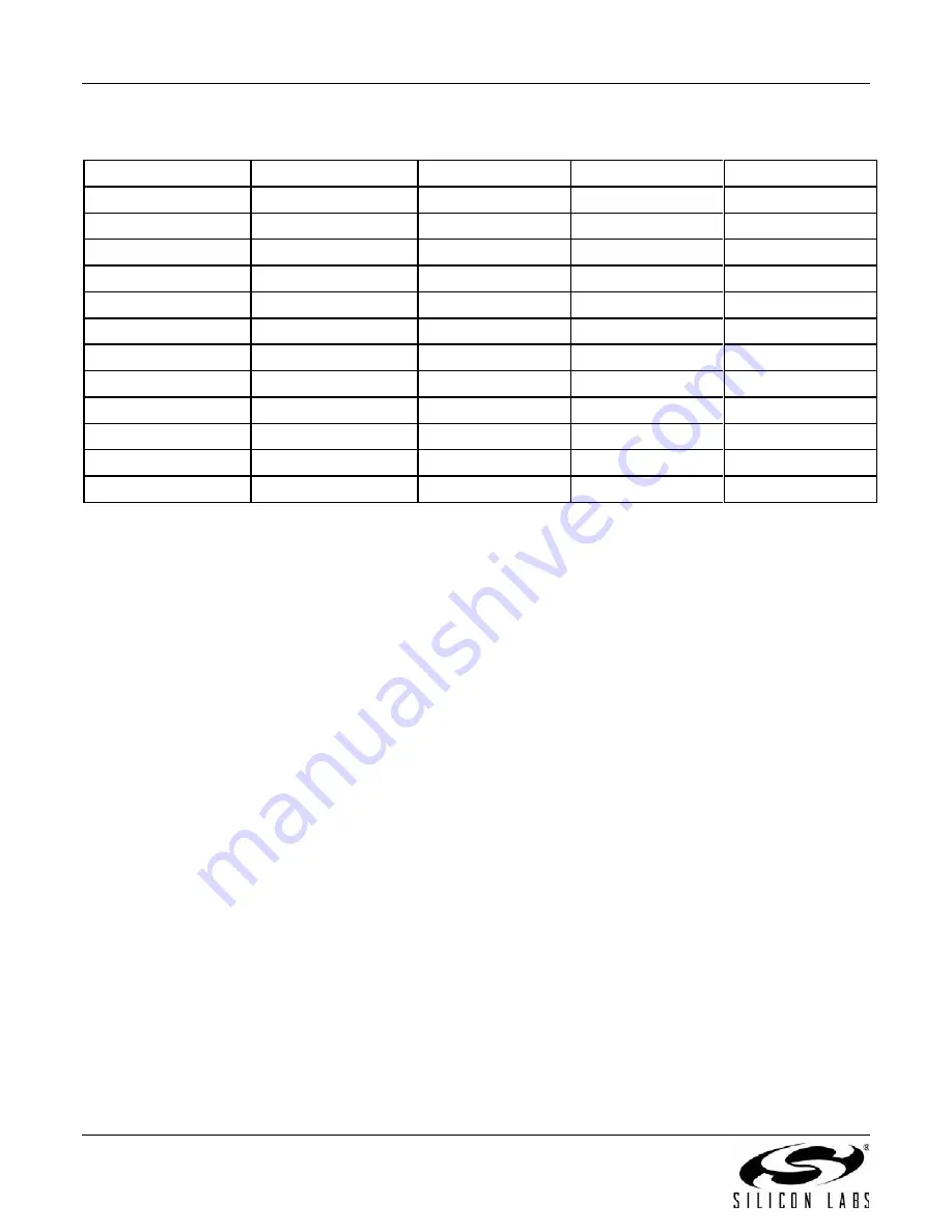
Table 11-3 shows the typical configurations of ADC inputs.
Table 11-3. Typical ADC Input Configurations
ADC P input
ADC N input
ADC_MUXP
ADC_MUXN
Purpose
ADC0
VREF/2
0
9
Single-ended
ADC1
VREF/2
1
9
Single-ended
ADC2
VREF/2
2
9
Single-ended
ADC3
VREF/2
3
9
Single-ended
ADC4
VREF/2
4
9
Single-ended
ADC5
VREF/2
5
9
Single-ended
ADC1
ADC0
1
0
Differential
ADC3
ADC2
3
2
Differential
ADC5
ADC4
5
4
Differential
GND
VREF/2
8
9
Calibration
VREF
VREF/2
10
9
Calibration
VDD_PADSA/2
VREF/2
11
9
Calibration
11.1.5.2 Input Range
The single-ended input range is fixed as 0 V to VREF and the differential input range is fixed as -VREF to +VREF.
11.1.5.3 Sample Time
ADC sample time is programmed by selecting the sampling clock and the clocks per sample.
The sampling clock may be either 1 MHz or 6 MHz. If the ADC_1MHZCLK bit in the ADC_CFG register is
clear, the 6 MHz clock is used; if it is set, the 1 MHz clock is selected. The 6 MHz sample clock offers faster
conversion times but the ADC resolution is lower than that achieved with the 1 MHz clock.
The number of clocks per sample is determined by the ADC_PERIOD bits in the ADC_CFG register.
ADC_PERIOD values select from 32 to 4096 sampling clocks in powers of two. Longer sample times produce
more significant bits. Regardless of the sample time, converted samples are always 16-bits in size with the
significant bits left-aligned within the value.
Summary of Contents for EMBER EM358 series
Page 2: ...EM358x 2 Rev 0 4 ...
Page 7: ...EM358x Rev 0 4 7 ...