CIRCUIT
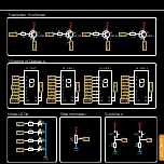
Circuit - Transistor Switches
When this Base Emitter (BE) current flows, it
will open the “gate” between the Collector and
Emitter (CE), allowing higher currents to flow
through the transistor. This then allows current
to flow through the 7-segment display’s com-
mon anode, and into any segments that are
currently pulled low. Thus, turning them on.
When the shift register pin is pulled high (fig.2),
there will be no potential difference between
the Emitter and the Base. So no current will
flow, and the “gate” will not open.
PNP Transistors
A Transistor can be used as a switch to apply
higher currents to a different part of the circuit
with only a small amount of current to trigger
it. This is perfect for our scenario, as the 595
Shift Register can’t source enough current to
power 8 LEDs on one output pin, or 32 LEDs
across 4 pins (our worst case scenario).
PNP Transistors turn on when a small amount
of current flows from Emitter to Base. When
enough flows from Emitter to Base, a much
greater current will flow from the Emitter to
the Collector. See the Component Index for
more info.
How the circuit works
In the circuit, when the Shift Registers output
pin is pulled low (fig.1), a small amount of cur-
rent flows from the Transistors Emitter to its
Base. Remember, conventional current flows
from positive to negative, if there is a poten-
tial difference between them. In our case, the
Emitter is at 5V and the Base (after a resistor)
is at 0V.
+5V
0V
0
PNP
E
Emitter
B
Base
C
Collector
GND
fig.1
+5V
+5V
1
E B
PNP
C
Emitter
Base
Collector
GND
fig.2
If none of the segments in the display are
pulled low, nothing will happen either, as there
will be no potential difference between the 5V
coming from the Transistor and the cathodes
of the display.
Switching
To use a Transistor as a switch, we need to
make sure the Transistor is in Saturation
Mode. For this we need to apply more than
enough current to the Base to ensure the Tran-
sistor switches on fully.
To calculate the Base Resistor value, we need
to know a few things. Firstly, how much cur-
rent will flow through the Transistor and the
display. We also need to know the Current
Gain (h
FE
)
We will be using 5mA of current per segment,
to stay within limits. If all of the segments were
on (showing an “8” and a decimal point), then
we would have 8 x 5mA flowing through the
Transistor. A total of 40mA. This would be
-40mA from the Shift Register’s point of view.
The 2N3906 is rated for -200mA, and the Shift
Register can take 6mA on each output, and
70mA total, so we are well within its limits.
As the Transistor is an amplifier, the current
gain (h
FE
) represents how many times the Base
current is amplified (multiplied) by, to equal the
Collector current. According to the datasheet,
at -50mA, this would be 60 times. So if we ap-
ply a 60th of the Collector Current to the Base,
it will turn the transistor on (when the Collector
Current is delivering around -50mA).
This would be the minimum amount of current
needed. Any fluctuations in temperature etc
would make this unreliable as a switch.
Q1-4
2N3906
R1-4
1.2K
DIGIT_4
DIGIT_3
DIGIT_2
DIGIT_1
+5V
1 1 0 0
On
On
Off
Off


