LTC3115-1
30
Rev. C
For more information
APPLICATIONS INFORMATION
PCB Layout Considerations
The LTC3115-1 buck-boost converter switches large cur-
rents at high frequencies. Special attention should be paid
to the PC board layout to ensure a stable, noise-free and
efficient application circuit. Figure 16 and Figure 17 show
a representative PCB layout for each package option to
outline some of the primary considerations. A few key
guidelines are provided below:
1. The parasitic inductance and resistance of all circulating
high current paths should be minimized. This can be
accomplished by keeping the routes to all bold compo-
nents in Figure 16 and Figure 17 as short and as wide
as possible. Capacitor ground connections should via
down to the ground plane by way of the shortest route
possible. The bypass capacitors on PV
IN
, PV
OUT
and
PV
CC
/V
CC
should be placed as close to the IC as possible
and should have the shortest possible paths to ground.
2. The exposed pad is the electrical power ground
connection for the LTC3115-1 in the DHD package.
Multiple vias should connect the backpad directly to
the ground plane. In addition, maximization of the met-
allization connected to the backpad will improve the
thermal environment and improve the power handling
capabilities of the IC in both the FE and DHD packages.
3. The components shown in bold and their connections
should all be placed over a complete ground plane to
minimize loop cross-sectional areas. This minimizes
EMI and reduces inductive drops.
4. Connections to all of the components shown in bold
should be made as wide as possible to reduce the
series resistance. This will improve efficiency and
maximize the output current capability of the buck-
boost converter.
5. To prevent large circulating currents in the ground plane
from disrupting operation of the LTC3115-1, all small-
signal grounds should return directly to GND by way
of a dedicated Kelvin route. This includes the ground
connection for the RT pin resistor, and the ground con-
nection for the feedback network as shown in Figure 16
and Figure 17.
6. Keep the routes connecting to the high impedance,
noise sensitive inputs FB and RT as short as possible
to reduce noise pick-up.
7. The BST1 and BST2 pins transition at the switching
frequency to the full input and output voltage respec-
tively. To minimize radiated noise and coupling, keep
the BST1 and BST2 routes as short as possible and
away from all sensitive circuitry and pins (VC, FB, RT).
In many applications the length of traces connecting to
the boost capacitors can be minimized by placing the
boost capacitors on the back side of the PC board and
routing to them via traces on an internal copper layer.
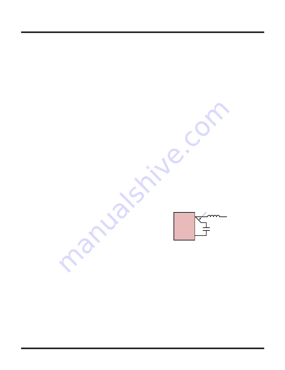
8 Connections from the BST1 and BST2 capacitors must
Kelvin directly back to the respective SW pin as shown
in Figure 15.
THIS ROUTE MUST KELVIN CONNECT
DIRECTLY BACK TO THE SW2 PIN
0.1µF
31151 F15
SW2
LTC3115-1
BST2
Figure 15. Kelvin BST Connections
9. If the optional Schottky diode from SW2 to PV
OUT
is
utilized, the Schottky should be placed as close to the
SW2 and PV
OUT
pins as possible and connected with
the shortest possible traces.


