


LTC3115-1
28
Rev. C
For more information
APPLICATIONS INFORMATION
Assuming a multiple of 50 separation between the pole
frequencies and zero frequencies this can be simplified
to the following expression:
G
CENTER
= 20log
50
2πf
C
R
TOP
C
FB
dB
This equation completes the set of constraints needed
to determine the compensation component values.
Specifically, the two zeros, f
ZERO1
and f
ZERO2
, should be
located near 3.43kHz. The two poles, f
POLE2
and f
POLE3
,
should be located near 168kHz and the gain should be set
to provide a gain at the crossover frequency of G
CENTER
= –19dB.
The first step in defining the compensation component
values is to pick a value for R
TOP
that provides an accept-
ably low quiescent current through the resistor divider.
A value of R
TOP
= 1MΩ is a reasonable choice. Next, the
value of C
FB
can be found in order to set the error ampli-
fier gain at the crossover frequency to –19dB as follows:
G
CENTER
= –19.1dB
= 20log
50
2π 24kHz
(
)
1MΩ
(
)
C
FB
C
FB
=
50
2π 24kHz
(
)
1MΩ
(
)
alog –19.1
20
≅
3.0nF
The compensation poles can be set at 168kHz and the
zeros at 3.43kHz by using the expressions for the pole
and zero frequencies given in the previous section. Setting
the frequency of the first zero, f
ZERO1
, to 3.43kHz results
in the following value for R
FB
:
R
FB
=
1
2π 3nF
(
)
3.43kHz
(
)
≅
15.4kΩ
This leaves the free parameter, C
POLE
, to set the frequency
f
POLE1
to the common pole frequency of 168kHz as given:
C
POLE
=
1
2π 15.4kΩ
(
)
168kHz
(
)
≅
62pF
Next, C
FF
can be chosen to set the second zero, f
ZERO2
, to
the common zero frequency of 3.43kHz.
C
FF
=
1
2π 1M Ω
(
)
3.43kHz
(
)
≅
47 pF
Finally, the resistor value R
FF
can be chosen to place the
second pole at 168kHz.
R
FF
=
1
2π 47pF
(
)
168Hz
(
)
≅
20.0kΩ
Now that the pole frequencies, zero frequencies and gain
of the compensation network have been established, the
next step is to generate a Bode plot for the compensated
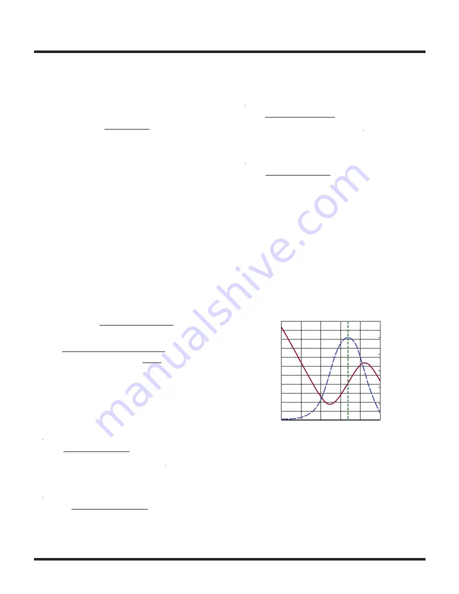
error amplifier to confirm its gain and phase properties.
A Bode plot of the error amplifier with the designed com-
pensation component values is shown in Figure 13. The
Bode plot confirms that the peak phase occurs at 24kHz
and the phase boost at that point is 57.7°. In addition,
the gain at the peak phase frequency is –19.3dB which is
close to the design target.
FREQUENCY (Hz)
10
–40
GAIN (dB)
PHASE (DEG)
–30
–20
–10
0
100
1k
10k
100k
3115 F13
1M
10
–35
–25
–15
–5
5
15
–90
f
C
–60
–30
0
30
60
GAIN
PHASE
90
Figure 13. Compensated Error Amplifier Bode Plot


