


LTC3115-1
29
Rev. C
APPLICATIONS INFORMATION
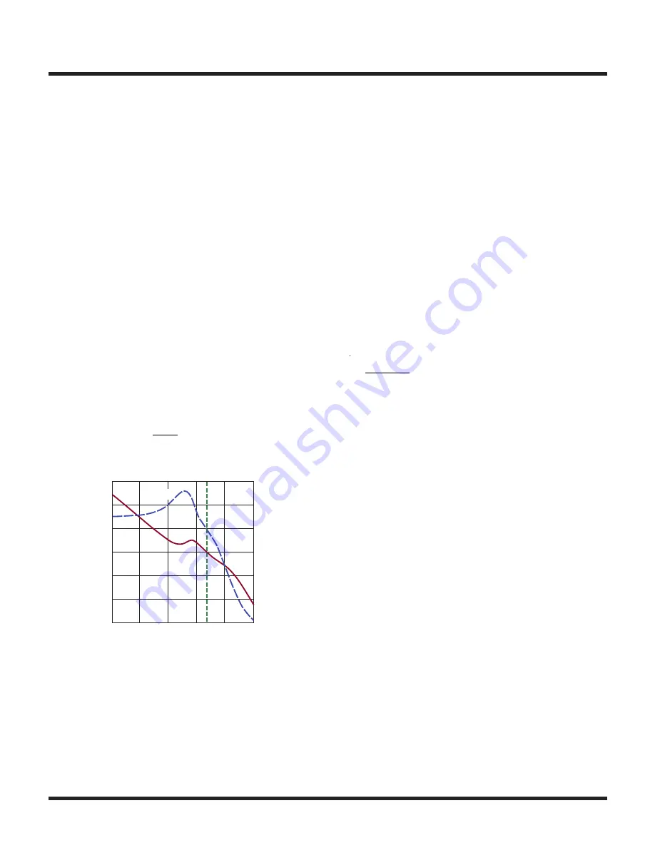
The final step in the design process is to compute the
Bode plot for the entire loop using the designed com-
pensation network and confirm its phase margin and
crossover frequency. The complete loop Bode plot for
this example is shown in Figure 14. The loop crossover
frequency is 22kHz which is close to the design target and
the phase margin is approximately 60°.
The Bode plot for the complete loop should be checked
over all operating conditions and for variations in compo-
nent values to ensure that sufficient phase margin exists
in all cases. The stability of the loop should also be con-
firmed via time domain simulation and by evaluating the
transient response of the converter in the actual circuit.
Output Voltage Programming
The output voltage is set via the external resistor divider
comprised of resistors R
TOP
and R
BOT
and Figure 9. The resistor divider values determine the
output regulation voltage according to:
V
OUT
= 1.000V 1+
R
TOP
R
BOT
Figure 14. Complete Loop Bode Plot
FREQUENCY (Hz)
10
–60
GAIN (dB)
PHASE (DEG)
–40
–20
0
20
40
60
–180
f
C
–120
–60
0
60
GAIN
120
180
100
1k
10k
100k
31151 F14
1M
PHASE
In addition to setting the output voltage, the value of
R
TOP
is instrumental in controlling the dynamics of the
compensation network. When changing the value of this
resistor, care must be taken to understand the impact this
will have on the compensation network.
In addition, the Thevenin equivalent resistance of the
resistor divider controls the gain of the current limit. To
maintain sufficient gain in this loop, it is recommended
that the value of R
TOP
be chosen to be 1MΩ or larger.
Switching Frequency Selection
The switching frequency is set by the value of a resistor
connected between the RT pin and ground. The switching
frequency, f, is related to the resistor value by the follow-
ing equation where R
T
is the resistance:
f =
35.7MHz
R
T
/ kΩ
(
)
Higher switching frequencies facilitate the use of smaller
inductors as well as smaller input and output filter capaci-
tors which results in a smaller solution size and reduced
component height. However, higher switching frequencies
also generally reduce conversion efficiency due to the
increased switching losses.
In addition, higher switching frequencies (above 750kHz)
will reduce the maximum output current that can be sup-
plied (see Typical Performance Characteristics for details).
For applications with V
OUT
≥ 20V, a maximum switching
frequency of 1MHz is recommended.


