


LTC3115-1
22
Rev. C
For more information
APPLICATIONS INFORMATION
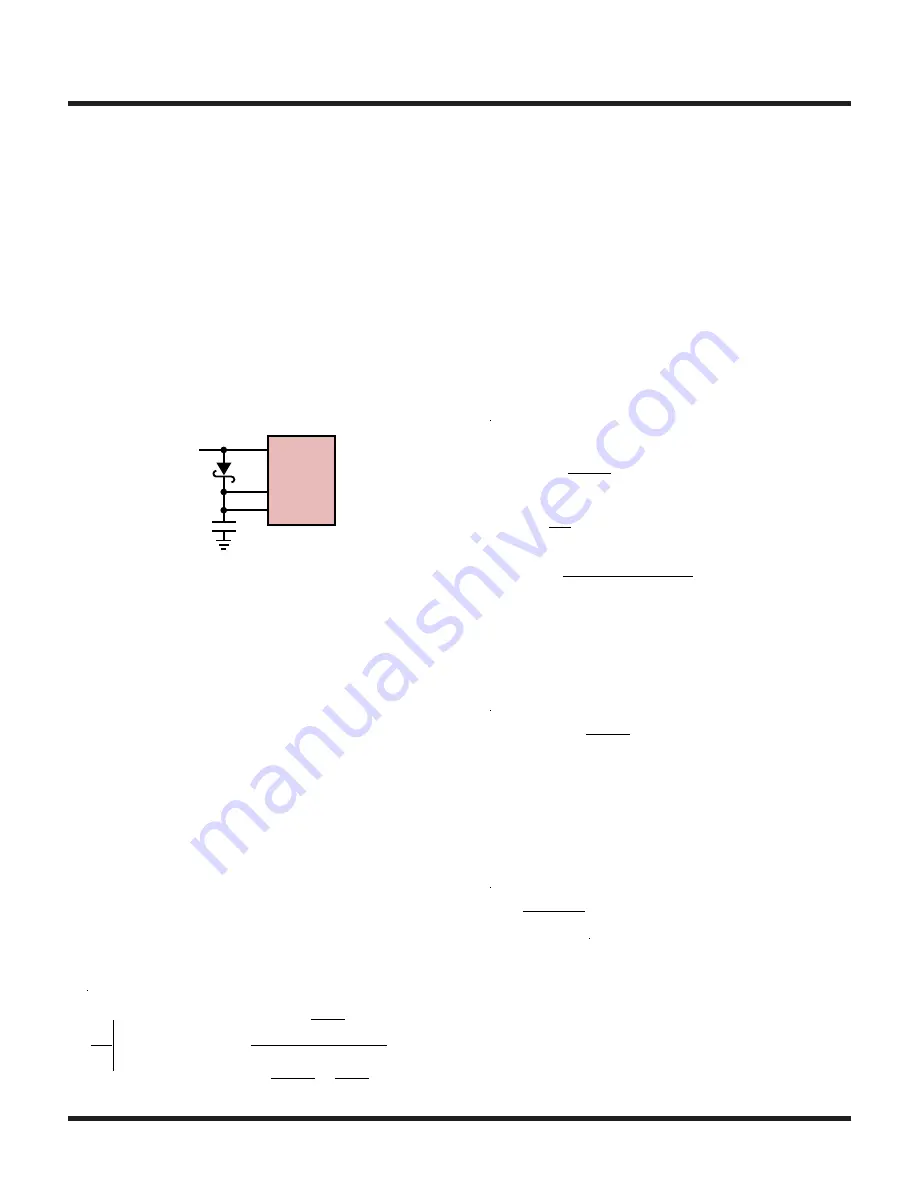
A significant performance advantage can be attained in
applications which have the converter output voltage pro-
grammed to 5V if the output voltage is utilized to power
the PV
CC
and V
CC
rails. This can be done by connect-
ing a Schottky diode from V
OUT
to PV
CC
/V
CC
as shown
in Figure 6. With this bootstrap diode installed, the gate
driver currents are generated directly by the buck-boost
converter at high efficiency rather than through the inter-
nal linear regulator. To minimize current drawn from the
output, the internal V
CC
regulator contains reverse block-
ing circuitry which minimizes the current into the PV
CC
/
V
CC
pins when they are driven above the input voltage.
The gain term, G
BUCK
, is comprised of three different com-
ponents: the gain of the analog divider, the gain of the pulse
width modulator, and the gain of the power stage as given
by the following expressions where V
IN
is the input voltage
to the converter, f is the switching frequency, R is the load
resistance, and t
LOW
is the switch pin minimum low time.
Curves showing the switch pin minimum low time can be
found in the Typical Performance Characteristics section of
this data sheet. The parameter R
S
represents the average
series resistance of the power stage and can be approxi-
mated as twice the average power switch resistance plus
the DC resistance of the inductor.
G
BUCK
= G
DIVIDER
G
PWM
G
POWER
G
DIVIDER
=
19.8V
V
IN
G
PWM
=
3
2V
1– t
LOW
f
(
)
G
POWER
=
V
IN
R
1– t
LOW
f
(
)
R +R
S
(
)
Notice that the gain of the analog divider cancels the input
voltage dependence of the power stage. As a result, the
buck mode gain is well approximated by a constant as
given by the following equation:
G
BUCK
= 29.7
R
R +R
S
≅
29.7 = 29.5dB
The buck mode transfer function has a single zero which
is generated by the ESR of the output capacitor. The zero
frequency, f
Z
, is given by the following expression where
R
C
and C
O
are the ESR and value of the output filter capac-
itor respectively.
f
Z
=
1
2π R
C
C
O
In most applications, an output capacitor with a very low
ESR is utilized in order to reduce the output voltage ripple
to acceptable levels. Such low values of capacitor ESR
result in a very high frequency zero and as a result the
zero is commonly too high in frequency to significantly
impact compensation of the feedback loop.
Figure 6. Bootstrapping PV
CC
and V
CC
V
OUT
4.7µF
31151 F06
PV
OUT
LTC3115-1
V
CC
PV
CC
Buck Mode Small-Signal Model
The LTC3115-1 uses a voltage mode control loop to
maintain regulation of the output voltage. An externally
compensated error amplifier drives the VC pin to generate
the appropriate duty cycle of the power switches. Use of
an external compensation network provides the flexibility
for optimization of closed loop performance over the wide
variety of output voltages, switching frequencies, and
external component values supported by the LTC3115-1.
The small-signal transfer function of the buck-boost con-
verter is different in the buck and boost modes of opera-
tion and care must be taken to ensure stability in both
operating regions. When stepping down from a higher
input voltage to a lower output voltage, the converter
will operate in buck mode and the small-signal transfer
function from the error amplifier output, V
C
, to the con-
verter output voltage is given by the following equation:
V
O
V
C BUCK MODE
=G
BUCK
1+ s
2πf
Z
1+
s
2πf
O
Q
+
s
2πf
O
2


