Chapter 5---Electronics
Model 250 Service Manual
5-25
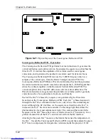
Horizontal Vertical Deflection PCB - Operation
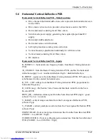
The Horizontal Vertical Deflection PCB consists of a RGB horizontal deflection
amplifier and separate vertical deflection amplifiers.
The Horizontal Deflection Amplifier
The horizontal deflection amplifier is a switching mode power supply that varies
according to the input horizontal sync frequency. The horizontal supply generates
the sawtooth current-driven waveform that drives the horizontal deflection coils
on the CRT. The sawtooth current waveform creates the raster on the CRT. The
horizontal amplifier also generates the retrace waveform portion of the raster.
The horizontal deflection sawtooth waveform is modulated by other waveforms
that perform geometric correction such as Pincushion, Keystone, Horizontal
Centering, Horizontal Linearity and Horizontal Width adjustment. The Width
Control voltage also goes to the Convergence Deflection PCB to adjust the
geometric correction parabolas.
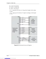
The H_F2V signal converts the input horizontal scan frequency to a voltage that
switches from one band (see explanation of bands in the Raster Timing Generator
PCB Operation section) to the next depending on the horizontal scan frequency.
This adjusts the retrace time to correspond to the input horizontal frequency. The
output of the horizontal supply is H_OUT_SUPPLY that goes on to the Scan
Reversal PCB.
CRT Protection
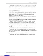
The Horizontal Vertical Deflection PCB uses the , H_LOCK- and
DEFL_OK signal to protect the CRTs from being damaged if the deflection
waveforms are lost. Refer to the CRT Protection section in Chapter 9 for a
complete discussion of these and all the signals associated with CRT Protection.
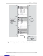
The Horizontal Vertical Deflection PCB receives the DEFL_OK signal from the
Scan Reversal PCB indicating the presence of the horizontal and vertical
deflection waveforms. If there is a failure of any of the Deflection Yokes
(horizontal or vertical), a current sense line on the Scan Reversal PCB forces
DEFL_OK low. On the Horizontal Vertical Deflection PCB, the DEFL_OK
signal becomes /SWEEP_OK and is sent to the Video Amplifier PCB where it
shuts down G
1
. If DEFL_Ok is forced low, or if /H_ENA is forced high,
/SWEEP_OK goes high. The /SWEEP_OK goes to the Video Amplifier PCB. If it
goes high, it shuts down the G
1
voltages and G
2
Regulator circuit (see
Troubleshooting, CRT Protection section).
Vertical Deflection Amplifier
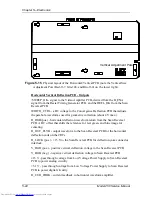
The vertical deflection sawtooth waveform is generated on the Convergence
Deflection PCB and timed to the vertical sync by the V_DRIVE signal from the
Raster Timing Generator PCB. The Convergence Deflection PCB sends this
waveform along with a parabola waveform V_PARAB to the vertical deflection
amplifier on the Horizontal Vertical Deflection PCB. The Horizontal Vertical
Deflection PCB takes V_RAMP, amplifies it and adds geometric correction with
Summary of Contents for 250
Page 16: ...Chapter 2 System Description Model 250 Service Manual 2 9 ...
Page 43: ...Chapter 4 Optical 4 10 Model 250 Service Manual Figure 4 6 Optical Path ...
Page 55: ...Chapter 5 Optical 3 4 22 Model 100 Service Manual ...
Page 91: ...Chapter 5 Electronics 5 36 Model 250 Service Manual Figure 5 22 Scan Reversal PCB I O Diagram ...
Page 131: ...Chapter 5 Electronics 5 76 Model 250 Service Manual Figure 5 44 Backplane Diagram right side ...
Page 132: ...Chapter 5 Electronics Model 250 Service Manual 5 77 ...
Page 138: ...Chapter 6 Miscellaneous Items 6 6 Model 250 Service Manual ...
Page 167: ...Chapter 7 Troubleshooting Model 250 Service Manual 7 29 ...
Page 181: ...Chapter 8 Software and Protocol 8 14 Model 250 Service Manual ...
Page 185: ...Chapter 9 Parts List 9 4 Model 250 Service Manual ...

