891
Chapter 44 A/D Converter
3.Registers of A/D Converter
Cleared by writing "0" or by a reset. (Not cleared at the end of DMA transfer.) However when waiting
condition of DMA transfer, this bit cannot be cleared.
Regarding protect function of converted data, see Section “
4. Operation of A/D Converter
".
[bit 3, 2] STS1, STS0 (Start source select)
These bits initialized "00" by reset.
These bits select the A/D activation source.
In multiple-activation modes, the first activation to occur starts A/D conversion.
The activation source changes immediately on writing to the register. Therefore care is required when
switching activation mode during A/D operation.
The A/D converter detects falling edges on the external trigger pin. When external trigger level is "L" and
if these bits are changed to external trigger activation mode, A/D converting may starts.
Selecting the timer selects the 16-bit reload timer 7.
[bit 1] STRT (Start)
Writing "1" to this bit starts A/D conversion (software activation).
Write "1" again to restart conversion.
Initialized to "0" by a reset.
In continuous and stop mode, restarting is not occurred. Check BUSY bit before writing "1". (Activate
conversion after clearing.)
Do not specify forcible termination and software activation (BUSY="0" and STRT="1") at the same time.
[bit 0] reserved bit
Always write "0" to this bit.
■
A/D control status register 0 (ADCS0)
• ADCS0 (ADC0): Address 01A5h (Access:
Half-word, Byte
)
(See “
Meaning of Bit Attribute Symbols (Page No.10)
” for details of the attributes.)
[bit 7, 6] MD1, MD0 (A/D converter mode set)
These bits the operation mode.
Single mode: Continuous A/D conversion from selected channel(s) ANS4 to ANS0 to selected channel(s)
ANE4 to ANE0 with a pause after every conversion cycle.
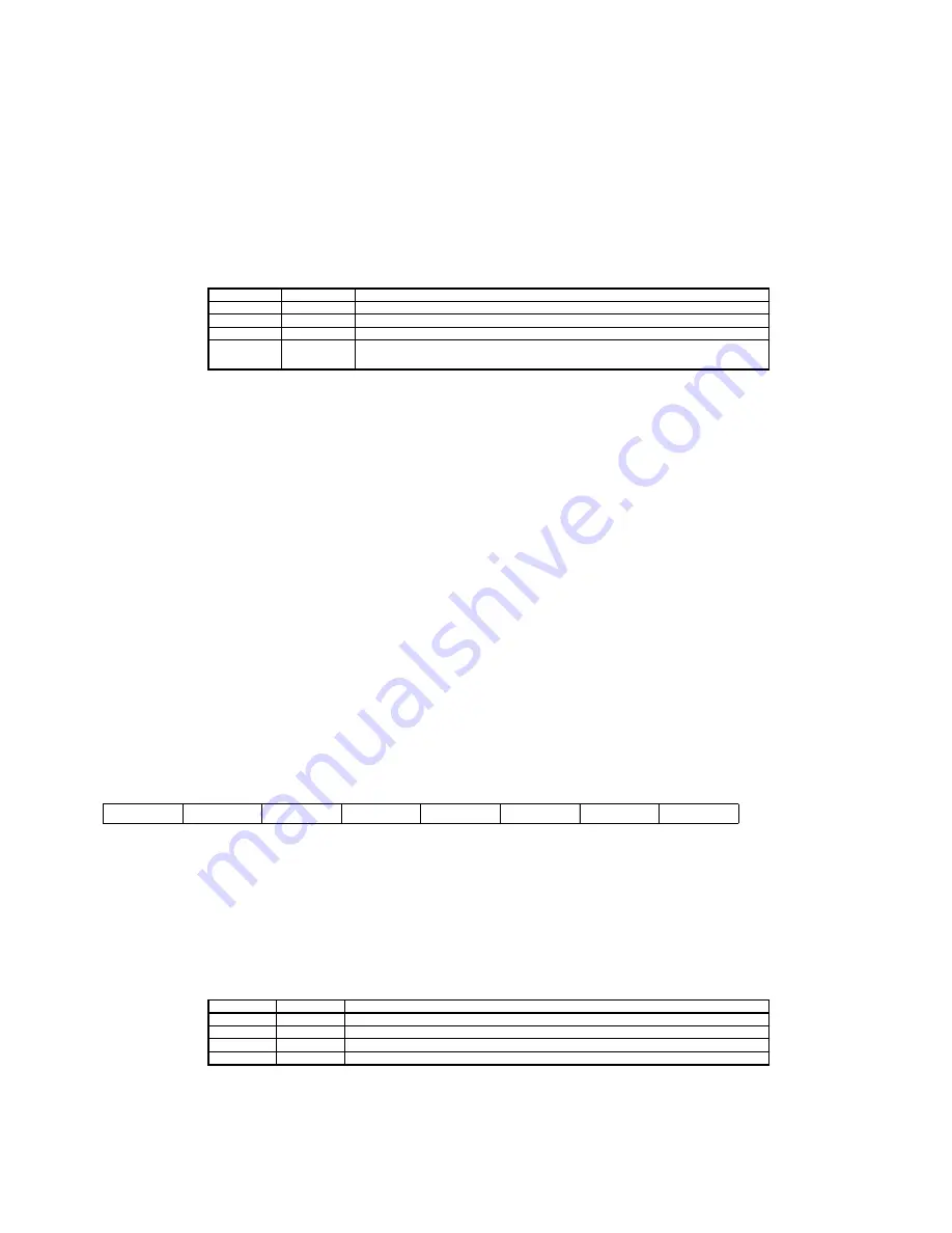
STS1
STS0
Function
0
0
Software activation [Initial value]
0
1
External trigger pin activation and software activation
1
0
Timer activation and software activation
1
1
External trigger pin activation, timer activation and software
activation
7
6
5
4
3
2
1
0
Bit
MD1
MD0
S10
ACH4
ACH3
ACH2
ACH1
ACH0
0
0
0
0
0
0
0
0
Initial
value
R/W
R/W
R/W
R
R
R
R
R
Attribute
MD1
MD0
Operating mode
0
0
Single mode ; all restarts conversion during operation enabled
0
1
Single mode ; restarts conversion during operation disabled
1
0
Continuous mode ; restarts conversion during operation disabled
1
1
Stop mode ; restarts conversion during operation disabled
Summary of Contents for FR Family FR60 Lite
Page 2: ...FUJITSU LIMITED ...
Page 3: ...FR60 32 BIT MICROCONTROLLER MB91460 Series User s Manual ...
Page 15: ...xi ...
Page 16: ...xii ...
Page 38: ...22 Chapter 2 MB91460 Rev A Rev B Overview 4 Block Diagram ...
Page 128: ...112 Chapter 4 CPU Architecture 9 Addressing ...
Page 153: ...137 Chapter 8 Device State Transition 3 State Transition Diagram ...
Page 154: ...138 Chapter 8 Device State Transition 3 State Transition Diagram ...
Page 169: ...153 Chapter 9 Reset 10 Caution ...
Page 170: ...154 Chapter 9 Reset 10 Caution ...
Page 180: ...164 Chapter 10 Standby 7 Q A ...
Page 182: ...166 Chapter 10 Standby 8 Caution ...
Page 199: ...183 Chapter 12 Instruction Cache 2 Main body structure Figure 2 3 I Cache Address Map ...
Page 200: ...184 Chapter 12 Instruction Cache 2 Main body structure Figure 2 4 I Cacheable Area ...
Page 222: ...206 Chapter 13 Clock Control 8 Caution ...
Page 232: ...216 Chapter 14 PLL Interface 7 Caution ...
Page 236: ...220 Chapter 15 CAN Clock Prescaler 3 Registers ...
Page 288: ...272 Chapter 19 Timebase Timer 8 Caution ...
Page 314: ...298 Chapter 22 Main Oscillation Stabilisation Timer 8 Caution ...
Page 326: ...310 Chapter 23 Sub Oscillation Stabilisation Timer 8 Caution ...
Page 348: ...332 Chapter 25 External Interrupt 8 Caution ...
Page 398: ...382 Chapter 26 DMA Controller 6 DMA External Interface ...
Page 402: ...386 Chapter 27 Delayed Interrupt 8 Caution ...
Page 412: ...396 Chapter 28 Bit Search 8 Caution ...
Page 521: ...505 Chapter 30 I O Ports 3 Port Register Settings ...
Page 522: ...506 Chapter 30 I O Ports 3 Port Register Settings ...
Page 574: ...558 Chapter 31 External Bus 4 Endian and Bus Access Byte Access ...
Page 628: ...612 Chapter 31 External Bus 13 Notes on Using the External Bus Interface ...
Page 706: ...690 Chapter 33 I2C Controller 4 Programming Flow Charts ...
Page 748: ...732 Chapter 34 CAN Controller 4 CAN Application ...
Page 762: ...746 Chapter 35 Free Run Timer 8 Caution ...
Page 790: ...774 Chapter 37 Output Compare 8 Caution ...
Page 838: ...822 Chapter 39 Programmable Pulse Generator 8 Caution ...
Page 850: ...834 Chapter 40 Pulse Frequency Modulator 4 PFM Operation and Setting ...
Page 886: ...870 Chapter 42 Sound Generator 3 Registers ...
Page 900: ...884 Chapter 43 Stepper Motor Controller 4 Caution ...
Page 939: ...923 Chapter 47 LCD Controller 3 Configuration Figure 3 2 Register List ...
Page 943: ...927 Chapter 47 LCD Controller 4 Registers Correspondence between VRAM and Common Segment Pins ...
Page 964: ...948 Chapter 48 Clock Monitor 8 Caution ...
Page 994: ...978 Chapter 51 Low Voltage Reset Interrupt 3 Registers ...
Page 998: ...982 Chapter 52 Regulator Control 3 Registers ...
Page 1008: ...992 Chapter 53 Fixed Mode Reset Vector BOOT ROM 5 Bootloader Update Strategy ...
Page 1024: ...1008 Chapter 54 Flash Memory 8 Caution ...
Page 1032: ...1016 Chapter 55 Flash Security 4 Register ...
Page 1034: ...1018 Chapter 56 Electrical Specification ...
Page 1035: ...FR60 MB91460 Series Hardware Manual European Microcontroller Design Centre Author MBo ...
Page 1036: ......
Page 1038: ......