


Epson Research and Development
Page 25
Vancouver Design Center
Hardware Functional Specification
SED1352
Issue Date: 99/07/28
X16-SP-001-16
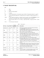
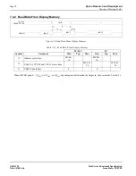
5.1 Summary of Configuration Options
The SED1352 requires some configuration information on power-up. This information is provided through the SRAM data
lines VD[0...15]. The state of these pins are read on the falling edge of RESET and used to configure the following options:
Note
The SED1352 has internal pulldown resistors on these pins and therefore will be pulled down
and read on a logic “0” after RESET. If pullup resistors are required refer to Table 6-3, “Input
Specifications,” on page 26 for pulldown resistor values.
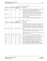
Example: If an ISA bus (no byte swap) with memory segment A000h and I/O location 300h are used, the corresponding
settings of VD15-VD0 would be:
Where x = don’t care; 1 = connected to pull-up resistor; 0 = no pull-up resistor.
Table 5-6: Summary of Power On / Reset Options
Pin Name
value on this pin at falling edge of RESET is used to configure:
(1/0)
1 0
VD0
16-bit host bus interface
8-bit host bus interface
VD1
Use direct-mapping for I/O accesses
Use internal index register for I/O accesses
VD2
MC68000 MPU interface
MPU / Bus interface with memory accesses
controlled by a READY (WAIT#) signal
VD3
Swap of high and low data bytes in 16-bit bus
interface
No byte swap of high and low data bytes in
16-bit bus interface
VD4-VD12
Select I/O mapping address bits [1:9].
These nine bits are latched on power-up and are compared to the MPU address bits [1-9]. A
valid I/O cycle combined with a valid address will enable the internal I/O decoder. Therefore,
both types of I/O mapping are limited to even address boundaries to determine either the
absolute or indexed I/O address of the first register. Note that a “valid I/O cycle” includes
IOCS# being toggled low.
In direct mapping, the base I/O address is selected by VD7-VD12. In indexing, the base I/O
address is selected by VD4-VD12.
VD13-VD15
Select memory mapping address bits [1:3].
These three bits are latched on power-up and are compared to the MPU address bits [17-19]. A
valid memory cycle combined with a valid address will enable the internal memory decoder.
As only the three most significant bits of the address are compared, the maximum amount of
memory supported is 128K bytes. Note that a “valid memory cycle” includes MEMCS# being
toggled low.
If 128K byte memory is used, it must be mapped at an even address so all 128K bytes is
available without a change in state on A17, as this would invalidate the internal compare logic.
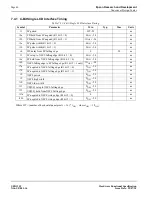
Table 5-7: I/O and Memory Addressing Example
8-Bit ISA Bus
16-Bit ISA Bus
Pin Name
Index
Register
Direct Mapping
Index
Register
Direct Mapping
VD0
0
0
1
1
VD1
0 1
0
1
VD2
0
0
0
0
VD3
0
0
0
0
VD12-VD4
11 0000 000
11 0000 xxx
11 0000 000
11 0000 xxx
VD15-VD13
101
101
101
101