


Page 10
Epson Research and Development
Vancouver Design Center
SED1352
SDU1352B0C Rev. 1.0 Evaluation Board User Manual
X16-AN-002-09
Issue Date: 98/10/07
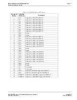
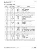
CPU / BUS Interface Connector Pinouts
Table 1-5: CPU/BUS Connector H1 Pinout
Connector
Pin No.
CPU/BUS
Pin Name
Comments
1
SD0
Connected to DB0 of the SED1352
2
SD1
Connected to DB1 of the SED1352
3
SD2
Connected to DB2 of the SED1352
4
SD3
Connected to DB3 of the SED1352
5
GND
Ground
6
GND
Ground
7
SD4
Connected to DB4 of the SED1352
8
SD5
Connected to DB5 of the SED1352
9
SD6
Connected to DB6 of the SED1352
10
SD7
Connected to DB7 of the SED1352
11
GND
Ground
12
GND
Ground
13
SD8
Connected to DB8 of the SED1352
14
SD9
Connected to DB9 of the SED1352
15
SD10
Connected to DB10 of the SED1352
16
SD11
Connected to DB11 of the SED1352
17
GND
Ground
18
GND
Ground
19
SD12
Connected to DB12 of the SED1352
20
SD13
Connected to DB13 of the SED1352
21
SD14
Connected to DB14 of the SED1352
22
SD15
Connected to DB15 of the SED1352
23
RESET
Connected to the RESET signal of the SED1352
24
GND
Ground
25
GND
Ground
26
GND
Ground
27
+12V
12 volt supply
28
+12V
12 volt supply
29
/SBHE
Connected to the BHE# signal of the SED1352
30
IOCHRDY Connected to the READY signal of the SED1352
31
/IOSC
Connected to the IOCS# signal of the SED1352
32
/MEMCS
Connected to the MEMCS# signal of the SED1352