


Epson Research and Development
Page 9
Vancouver Design Center
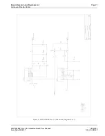
ISA Bus Interface Considerations
SED1352F0B
Issue Date: 98/10/08
X16-AN-003-05
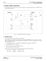
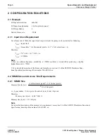
1.5 SED1352F0B Default Setup
1.5.1 Configuration Options
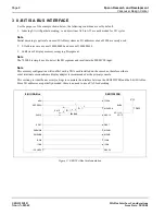
1.
VD15 - VD13 = 101
memory decoding for locations $A segment
2.
VD12 - VD4 = 110000000
I/O decoding for locations 1100000000b - 1100000001b
3.
VD3 = 0
No byte swap of high and low bytes
4.
VD2 = 0
ISA Bus interface, i.e. non- MC68K interface
5.
VD1 = 0
Indexing I/O
6.
VD0 = 0
8-bit bus interface
Where 1 = pull-up with a 10K resistor; 0 = no pull-up resistor
Note
The states of these data pins are internally latched during RESET.
1.5.2 Register Setting
AUX[1] bit 1 = 0 for 16-bit memory interface or
AUX[1] bit 1 = 1 for 8-bit memory interface.