


Page 8
Epson Research and Development
Vancouver Design Center
SED1352
SDU1352B0C Rev. 1.0 Evaluation Board User Manual
X16-AN-002-09
Issue Date: 98/10/07
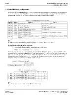
1.2 Installation and Configuration
The SED1352 has 16 configuration inputs (VD[15:0]) which are read on power-up. For the purpose of this design, most of
these configuration inputs have been factory set and therefore are not configurable. A four position DIP switch block is
provided for the selection of 8- or 16-bit bus interface, and setting I/O address bits 4 through 6.
Note
The polarity of the Configuration Dip Switches is Closed = ’1’ or ’high’, Open = ’0’ or ’low’.
Factory set fixed options on this board are:
•
16-bit display memory interface (either 64K bytes or 128K bytes)
•
128K bytes available at C000h memory segment
This board is also pre-set to use indexing I/O with address 0000 0011 0??? 000x, where x is don’t care and ??? can be
configured with dip-switch SW1-5 through SW1-7. The factory setting of ??? = 001, i.e., I/O address = 0310h and 0311h.
When using direct-mapping I/O, the I/O address is 0000 0011 0??? xxxx, where x is don’t care and ??? can be configured
with dip-switch SW1-5 through SW1-7. If ??? = 001, then the I/O address for AUX[00h ] = 0310h, I/O address for
AUX[01h] = 0311h, I/O address for AUX[02h] = 0312h and so on.
Note
These jumpers are necessary for the external ISA Bus decode logic.
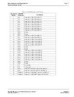
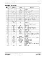
Table 1-1: Configuration DIP Switch Settings
Switch
Signal
Closed
Open
SW1-1
VD0
16-bit ISA Bus interface
8-bit ISA Bus interface
SW1-2
VD1
Direct-mapping I/O
Indexing I/O
SW1-3
VD2
M68K CPU Interface
ISA Bus / other MPU other
SW1-4
VD3
Byte-swap high and low data bytes
No byte-swap
SW1-5
VD7
I/O mapping address bit 4
See Table 1-2, “I/O Mapping Example”
SW1-6
VD8
I/O mapping address bit 5
SW1-7
VD9
I/O mapping address bit 6
SW1-8
-
64K bytes of SRAM available at segment
D000h
128K bytes of SRAM available at segment C000h-
D000h
Table 1-2: I/O Mapping Example
bit 6 bit 5 bit 4
I/O Mapping Address (Hex)
0
0
1
Table 1-3: Decoding Jumper Setting
Description
1-2
2-3
JP1
Set to the same polarity as SW1-1 (VD0)
1
0
JP2
Set to the same polarity as SW1-5 (VD7)
1
0
JP3
Set to the same polarity as SW1-6 (VD8)
1
0
JP4
Set to the same polarity as SW1-7 (VD9)
1
0