


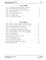


Page 8
Epson Research and Development
Vancouver Design Center
SED1352
Programming Notes and Examples
X16-BG-007-04
Issue Date: 98/10/08
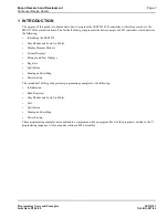
2 INITIALIZING THE SED1352
This section presents two examples to show how to initialize the SED1352 registers and write a pixel to the display. Code
to initialize the SED1352 is provided in Section 6.2, “Initialization Code” on page 48.
The following examples describe values written to registers.
•
A “normal” value is one which must not change after initialization of all registers.
•
A “panel specific” value is one required for the given type of panel. Such a value must never change after initializa-
tion of all registers.
•
An “implementation specific” value is one required for the hardware implementation of the SED1352. Such a value
must never change after initialization of all registers. Refer to the SED1352F0x Hardware Functional Specification
and SDU1352B0x Evaluation Board User’s Manual for more information on hardware implementation issues.
•
An “application specific” value is one that can be changed by the program after initialization of all registers.
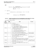
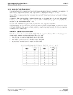
Example 1:
Initialize the registers for a 16 gray shade 320x240 single panel LCD with 64k of display
memory. Afterwards write one pixel to the top left corner of the display.
Program SED1352 Registers 00h-0Dh:
AUX
Register
Data
(in Binary)
Notes
See Also
AUX[00h]
0000 0000
•
must be zero
AUX[01h]
1000 1000
•
b7 = display on (normal)
•
b6 = single panel (panel specific)
•
b5 = XSCL not masked (panel specific)
•
b4 = LCDE LCDENB pin = 0 (implementation specific; the
recommended procedure is to turn this bit off during register
initialization and afterwards turn this bit on)
•
b3 = 16 grays (application specific)
•
b2 = 4 bit LCD data width (panel specific)
•
b1 = 16 bit Memory Interface (implementation specific)
•
b0 = RAMS ignored (implementation specific)
AUX[02h]
0100 1111
•
bits 7-0 = bits 7-0 of Line Byte Count (panel specific)
•
bit 8 of Line Byte Count in bit 0 of AUX[03h] (panel specific)
see Note A at end of
Table for calculation
AUX[03h]
0000 0110
•
bits 7-6 = Power Save Mode 0 (application specific)
•
bit 5 = LCD interface signals forced to 0 during Power Save
(implementation specific)
•
bit 4 = no LUT bypass (application specific)
•
bits 3-1 = not used
•
bit 0 = bit 8 of Line Byte Count (panel specific, see AUX[02h])
see Section 5.6, “Power
Saving” on page 44
AUX[04h]
1110 1111
•
bits 7-0 = bits 7-0 of Total Display Line Count (panel specific)
•
bits 9-8 of Total Display Line Count in bits 1-0 of AUX[05h]
(panel specific)
see Note B and C at end
of Table for calculation
AUX[05h]
0000 0000
•
bits 7-2 = WF not required (panel specific)
•
bits 1-0 = bits 9-8 of Total Display Line Count (panel specific,
see AUX[04h])