


Epson Research and Development
Page 9
Vancouver Design Center
SDU1352B0C Rev. 1.0 Evaluation Board User Manual
SED1352
Issue Date: 98/10/07
X16-AN-002-09
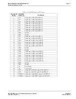
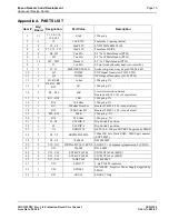
LCD Signal Connector Pinout
Table 1-4: LCD Signal Connector J1 Pinout
SED1352
Pin Name
LCD
Connector
Pin No.
Mono STN LCD
Comments
8-bit
4-bit
LD0
1
LD0
Lower panel display data for dual panel-dual drive
mode. In 8-bit single panel-single drive mode, these
are the least significant 4 bits of the 8-bit output data
to the panel (data[3:0]). In 4-bit single panel mode,
these outputs are low.
LD1
3
LD1
LD2
5
LD2
LD3
7
LD3
UD0
9
UD0
UD0
Upper panel display data for dual panel-dual drive
mode. In 8-bit single panel-single drive mode, these
are the most significant 4 bits of the 8-bit output data
to the panel (data[7:4]). In 4-bit single panel mode,
these are the 4 data bits output to the panel.
UD1
11
UD1
UD1
UD2
13
UD2
UD2
UD3
15
UD3
UD3
N/C
17-31
(odd pins)
XSCL
33
XSCL
XSCL
Shift Clock for LCD data
NC
35
LP
37
LP
LP
Latch Pulse output
YD
39
YD
YD
Vertical Scanning Start Pulse
GRND
2-26
(even pins)
GRND
GRND
Logic Ground
N/C
28
VLCD
30
VLCD
VLCD
Negative power supply output (-18V to -23V)
VCC
32
+5V
+5V
+12V
34
+12V
+12V
VDDH
36
VDDH
VDDH
Positive power supply output (+23V to +40V)
WF
38
WF
WF
LCD backplane Bias signal
LCDENB
40
/LCDPWR
/LCDPWR LCD power control to external supply