SIC63616-(Rev. 1.0) NO. P97
3240-0412
4.9 Programmable Timer
4.9.1 Configuration of programmable timer
The S1C63616 has built-in four (Ch.A–Ch.D) units of 8 bits × 2-channel programmable timers. Each unit
may be configured to 8-bit timer × 2 channels or 16-bit timer × 1 channel with software.
Ch.A: Timer 0 and Timer 1 (8 bits × 2 channels) or Timer 0 + 1 (16 bits x 1 channel)
Ch.B: Timer 2 and Timer 3 (8 bits × 2 channels) or Timer 2 + 3 (16 bits × 1 channel)
Ch.C: Timer 4 and Timer 5 (8 bits × 2 channels) or Timer 4 + 5 (16 bits × 1 channel)
Ch.D: Timer 6 and Timer 7 (8 bits × 2 channels) or Timer 6 + 7 (16 bits × 1 channel)
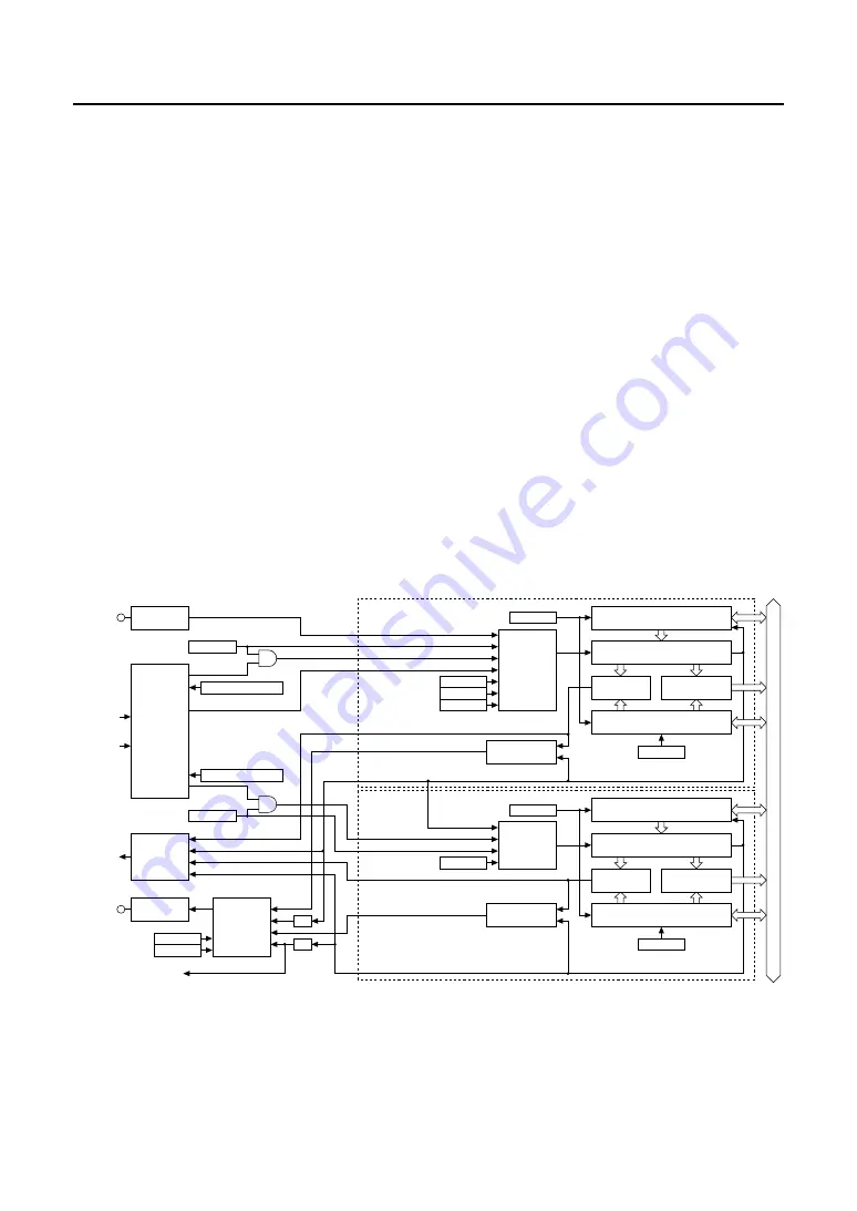
Figures 4.9.1.1 to 4.9.1.4 show the configuration of the programmable timers.
Each timer has an 8-bit down counter and an 8-bit reload data register. The down counter counts the
internal clock of which the frequency can be selected with software. Furthermore, Timers 0, 2, 4, 6 also have
an event counter function to count the clock input from the P12, P41, P42 and P43 terminals. When the
down counter underflows during counting with the specified clock, the timer outputs the underflow and
interrupt signals and resets the counter to its initial value. The reload data register is used to set that initial
value.
The underflow signal of Timer 1 is used as the source clock of the R/f converter and serial interface, this
makes it possible to program a flexible R/f converter count clock and the transfer rate of the serial interface.
Each timer has an 8-bit compare data register in addition to the above registers. This register is used to store
data to be compared with the contents of the down counter. When the timer is set to PWM mode, the timer
outputs the compare match signal if the contents between the down counter and the compare data register
are matched, and an interrupt occurs at the same time. Also the compare match signal is used with the
underflow signal to generate a PWM waveform.
The signal generated by the programmable timer can be output from the P13 port terminal.
Timer 0
Timer 0 clock selection
Underflow signal
Compare match signal
Interrupt
request
Timer 0 reset
Timer 0
clock
Timer 1
clock
PWM output selection
R/f converter
Serial interface
P12
PTSEL0
PTRST0
Data b
us
Timer 0
Run/Stop
PTRUN0
PTPS00–PTPS03
Timer function setting
f
OSC1
/16 (2,048 Hz)
f
OSC1
FCSEL_A
Timer 1 clock selection
PTPS10–PTPS13
f
OSC3
Pulse polarity setting
PLPUL_A
Output control
PTOUT_A
Output selection
CHSEL_A
Event counter
mode setting
EVCNT_A
Reload data register
RLD00–RLD07
Compare data register
CD00–CD07
8-bit down counter
Timer
control
circuit
PWM waveform
generator
P12 port
TOUT_A
(P13)
P13 port
Clock
manager
Interrupt
control
circuit
Selector
Data buffer
PTD00–PTD07
Comparator
Timer 1
Underflow signal
Compare match signal
Timer 1 reset
PWM output selection
PTSEL1
PTRST1
Timer 1
Run/Stop
PTRUN1
1/2
1/2
16-bit mode
selection
MOD16_A
Reload data register
RLD10–RLD17
Compare data register
CD10–CD17
8-bit down counter
Timer
control
circuit
PWM waveform
generator
Data buffer
PTD10–PTD17
Comparator
Fig. 4.9.1.1 Configuration of programmable timer Ch.A (Timers 0 and 1)


