


APPENDIX 3 FIRMWARE SWITCHS (WSW)
A-20
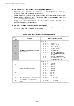
WSW13 (Modem setting)
Selector
No.
Function
Setting and Specifications
1
2
Cable equalizer
No. 1 2
0
0
:
0
km
0
1
:
1.8 km
1
0
: 3.6
km
1
1
: 5.6
km
3
4
Reception level
No. 3 4
0
0
:
-43
dBm
0
1
:
-47
dBm
1
0
:
-49
dBm
1
1
:
-51
dBm
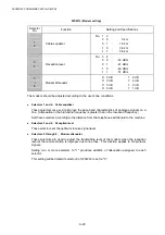
5
|
8
Modem attenuator
0: 0
dB
1: 8
dB
0: 0
dB
1: 4
dB
0: 0
dB
1: 2
dB
0: 0
dB
1: 1
dB
The modem should be adjusted according to the user's line conditions.
l
Selectors 1 and 2: Cable equalizer
These selectors are used to improve the pass-band characteristics of analogue signals on a
line. (Attenuation in the high-band frequency is greater than in the low-band frequency.)
Set these selectors according to the distance from the telephone switchboard to the machine.
l
Selectors 3 and 4: Reception level
These selectors set the optimum receive signal level.
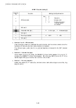
l
Selectors 5 through 8: Modem attenuator
These selectors are used to adjust the transmitting level of the modem when the reception
level at the remote station is improper due to line loss. This function applies to G3 protocol
signals.
Setting two or more selectors to "1" produces addition of attenuation assigned to each
selector.
This setting will be limited if selector 8 of WSW23 is set to "0."
Summary of Contents for DCP-8040
Page 276: ...CHAPTER 7 MAINTENANCE MODE 7 6 Fig 7 3 l m a b c d e f g h i j k ...
Page 347: ...APPENDIX 4 CIRCUIT DIAGRAMS A 50 Appendix 4 1 Main PCB Circuit Diagram 1 7 ...
Page 349: ...APPENDIX 4 CIRCUIT DIAGRAMS A 52 Appendix 4 3 Main PCB Circuit Diagram 3 7 ...
Page 351: ...APPENDIX 4 CIRCUIT DIAGRAMS A 54 Appendix 4 5 Main PCB Circuit Diagram 5 7 ...
Page 353: ...APPENDIX 4 CIRCUIT DIAGRAMS A 56 Appendix 4 7 Main PCB Circuit Diagram 7 7 ...
Page 355: ...APPENDIX 4 CIRCUIT DIAGRAMS A 58 Appendix 4 9 Engine PCB Circuit Diagram 1 2 ...
Page 357: ...APPENDIX 4 CIRCUIT DIAGRAMS A 60 Appendix 4 11 NCU PCB Circuit Diagram U S A ...
Page 359: ...APPENDIX 4 CIRCUIT DIAGRAMS A 62 Appendix 4 13 NCU PCB Circuit Diagram Asia ...
Page 361: ...APPENDIX 4 CIRCUIT DIAGRAMS A 64 Appendix 4 15 Control Panel PCB Circuit Diagram ...
Page 367: ...April 04 SM FAX027 5 8C5903 Printed in Japan ...