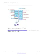
PAD SET 0
PAD SET 1
Offset
PAD
Offset
PAD
12
12.0 dB
12
spare
13
13.0 dB
13
spare
14
14.0 dB
14
Idle Code
15
spare
15
Unassigned Code
Signaling interface
The signaling interface consists of the A07 DS-30X signaling controller. This interface provides
an 8 Kbps signaling link through the DS-30X timeslot zero data bit zero. Messages are 3 bytes
in length.
Carrier interface
The E1 interface connection to the external digital carrier is provided by the line interface chip.
This chip provides accurate pulse shaping to meet the CCITT pulse mask requirements. It
provides clock recovery functions on the receive side as well as tolerance to jitter and wander
in the received bit stream.
Impedance matching
The line interface provides for the use of 120 ohms twisted pair cable. The impedance is
selected by a switch, as shown in
Table 232: Impedance matching switch selection
page 528.
Table 232: Impedance matching switch selection
Cable
On
Off
120 ohms
S1
S2
Note:
The ON position for all the switches is towards the bottom of the card. This is indicated by
a white dot printed on the board next to the bottom left corner of each individual switch.
Carrier grounding
The NTAK79 card provides the capability of selectively grounding the shield of the Tx and/or
Rx pairs of the carrier. Closing (down) the on-board switch applies FGND to the appropriate
NTAK79 2.0 Mb PRI card
528 Circuit Card Reference
July 2011
Summary of Contents for 1000 Series
Page 1: ...Circuit Card Reference Nortel Communication Server 1000 7 0 NN43001 311 04 04 July 2011 ...
Page 20: ...20 Circuit Card Reference July 2011 ...
Page 30: ...Introduction 30 Circuit Card Reference July 2011 Comments infodev avaya com ...
Page 116: ...Option settings 116 Circuit Card Reference July 2011 Comments infodev avaya com ...
Page 143: ...Figure 25 CP PIV card front Physical description Circuit Card Reference July 2011 143 ...
Page 148: ...NT4N39AA CP Pentium IV Card 148 Circuit Card Reference July 2011 Comments infodev avaya com ...
Page 287: ...Figure 86 Clock Controller Option 3 Operation Circuit Card Reference July 2011 287 ...
Page 302: ...NT5K21 XMFC MFE card 302 Circuit Card Reference July 2011 Comments infodev avaya com ...
Page 346: ...NT6D80 MSDL card 346 Circuit Card Reference July 2011 Comments infodev avaya com ...
Page 353: ...Figure 96 NTDK16 DLC Functional description Circuit Card Reference July 2011 353 ...
Page 461: ...Figure 147 Paging trunk operation Applications Circuit Card Reference July 2011 461 ...
Page 462: ...NT8D15 E and M Trunk card 462 Circuit Card Reference July 2011 Comments infodev avaya com ...
Page 500: ...NTAK09 1 5 Mb DTI PRI card 500 Circuit Card Reference July 2011 Comments infodev avaya com ...
Page 512: ...NTAK10 2 0 Mb DTI card 512 Circuit Card Reference July 2011 Comments infodev avaya com ...
Page 534: ...NTAK79 2 0 Mb PRI card 534 Circuit Card Reference July 2011 Comments infodev avaya com ...
Page 550: ...NTBK22 MISP card 550 Circuit Card Reference July 2011 Comments infodev avaya com ...
Page 560: ...NTBK50 2 0 Mb PRI card 560 Circuit Card Reference July 2011 Comments infodev avaya com ...
Page 595: ...Figure 165 MGC block diagram Introduction Circuit Card Reference July 2011 595 ...
Page 662: ...NTRB21 DTI PRI DCH TMDI card 662 Circuit Card Reference July 2011 Comments infodev avaya com ...
Page 668: ...NTVQ01xx Media Card 668 Circuit Card Reference July 2011 Comments infodev avaya com ...
Page 700: ......


