91
ATmega103(L)
0945G–09/01
serve this function. See the Timer/Counter1 description on how to operate this function.
The internal pull-up MOS resistor can be activated as described above.
• T1 – Port D, Bit 6
T1, Timer/Counter1 counter source. See the timer description for further details.
• T2 – Port D, Bit 7
T2, Timer/Counter2 counter source. See the timer description for further details.
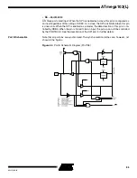
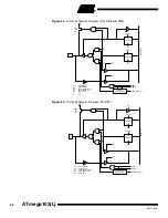
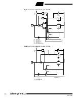
Port D Schematics
Note that all port pins are synchronized. The synchronization latches are, however, not
shown in the figures.
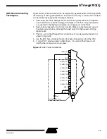
Figure 62.
Port D Schematic Diagram (Pins PD0, PD1, PD2 and PD3)
DA
T
A
B
U
S
D
D
Q
Q
RESET
RESET
C
C
WD
WP
RD
MOS
PULL-
UP
PDn
R
R
WP:
WD:
RL:
RP:
RD:
n:
WRITE PORTD
WRITE DDRD
READ PORTD LATCH
READ PORTD PIN
READ DDRD
0, 1, 2, 3
DDDn
PORTDn
INTn
RL
RP

