10
ATmega103(L)
0945G–09/01
X-register, Y-register and Z-
register
The registers R26..R31 have some added functions to their general-purpose usage.
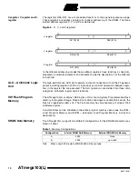
These registers are address pointers for indirect addressing of the SRAM. The three
indirect address registers X, Y, and Z are defined as:
Figure 6.
X-, Y-, and Z-registers
In the different addressing modes these address registers have functions as fixed dis-
placement, automatic increment and decrement (see the descriptions for the different
instructions).
ALU – Arithmetic Logic
Unit
The high-performance AVR ALU operates in direct connection with all the 32 general-
purpose working registers. Within a single clock cycle, ALU operations between regis-
ters in the register file are executed. The ALU operations are divided into three main
categories: arithmetic, logical and bit functions.
ISP Flash Program
Memory
The ATmega103(L) contains 128K bytes of On-chip In-System Programmable Flash
memory for program storage. Since all instructions are single or double 16-bit words, the
Flash is organized as 64K x 16. The Flash memory has an endurance of at least 1000
write/erase cycles.
Constant tables can be allocated in the entire program memory space (see the LPM –
Load Program Memory and ELPM – Extended Load Program Memory instruction
descriptions).
SRAM Data Memory
The ATmega103(L) supports two different configurations for the SRAM data memory as
listed in Table 1.
Note:
When using 64K of external SRAM, 60K will be available.
15
0
X-register
7 0
7 0
R27 ($1B)
R26 ($1A)
15
0
Y-register
7 0
7 0
R29 ($1D)
R28 ($1C)
15
0
Z-register
7 0
7 0
R31 ($1F)
R30 ($1E)
Table 1.
Memory Configurations
Configuration
Internal SRAM Data Memory
External SRAM Data Memory
A
4000
None
B
4000
up to 64K

