75
ATmega103(L)
0945G–09/01
ADC Noise Canceler
Function
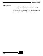
The ADC features a noise canceler that enables conversion during idle mode to reduce
noise induced from the CPU core. To make use of this feature, the following procedure
should be used:
1.
Turn off the ADC by clearing ADEN.
2.
Turn on the ADC and simultaneously start a conversion by setting ADEN and
ADSC. This starts a dummy conversion that will be followed by a valid
conversion.
3.
Within 14 ADC clock cycles, enter idle mode.
4.
If no other interrupts occur before the ADC conversion completes, the ADC inter-
rupt will wake up the MCU and execute the ADC conversion complete interrupt
routine.
ADC Multiplexer Select
Register – ADMUX
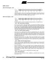
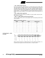
• Bits 7..3 – Res: Reserved Bits
These bits are reserved bits in the ATmega103(L) and always read as zero.
• Bits 2..0 – MUX2..MUX0: Analog Channel Select Bits 2 - 0
The value of these three bits selects which analog input 7 - 0 is connected to the ADC.
ADC Control and Status
Register – ADCSR
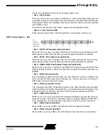
• Bit 7 – ADEN: ADC Enable
Writing a logical “1” to this bit enables the ADC. By clearing this bit to zero, the ADC is
turned off. Turning the ADC off while a conversion is in progress will terminate this
conversion.
• Bit 6 – ADSC: ADC Start Conversion
A logical “1” must be written to this bit to start each conversion. The first time ADSC has
been written after the ADC has been enabled, or if ADSC is written at the same time as
the ADC is enabled, a dummy conversion will precede the initiated conversion. This
dummy conversion performs initialization of the ADC.
ADSC remains high during the conversion. ADSC goes low after the conversion is com-
plete, but before the result is written to the ADC Data registers. This allows a new
conversion to be initiated before the current conversion is complete. The new conver-
sion will then start immediately after the current conversion completes. When a dummy
conversion precedes a real conversion, ADSC will stay high until the real conversion
completes.
Writing a zero to this bit has no effect.
• Bit 5 – Res: Reserved Bit
This bit is reserved in the ATmega103(L).
Warning:
When writing ADCSR, a logical “0”
must be written to this bit.
Bit
7
6
5
4
3
2
1
0
$07 ($27)
–
–
–
–
–
MUX2
MUX1
MUX0
ADMUX
Read/Write
R
R
R
R
R
R/W
R/W
R/W
Initial Value
0
0
0
0
0
0
0
0
Bit
7
6
5
4
3
2
1
0
$06 ($26)
ADEN
ADSC
–
ADIF
ADIE
ADPS2
ADPS1
ADPS0
ADCSR
Read/Write
R/W
R/W
R
R/W
R/W
R/W
R/W
R/W
Initial Value
0
0
0
0
0
0
0
0

