84
ATmega103(L)
0945G–09/01
Note:
n: 7,6...0, pin number
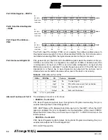
Alternate Functions of Port B
The alternate pin configuration is as follows:
• OC2/PWM2, Bit 7
OC2/PWM2, Output Compare output for Timer/Counter2 or PWM output when
Timer/Counter2 is in PWM Mode. The pin has to be configured as an output to serve
this function.
• OC1B/PWM1B, Bit 6
OC1B/PWM1B, Output Compare output B for Timer/Counter1 or PWM output B when
Timer/Counter1 is in PWM Mode. The pin has to be configured as an output to serve
this function.
• OC1A/PWM1A, Bit 5
OC1A/PWM1A, Output Compare output A for Timer/Counter1 or PWM output A when
Timer/Counter1 is in PWM Mode. The pin has to be configured as an output to serve
this function.
• OC0/PWM0, Bit 4
OC0/PWM0, Output Compare output for Timer/Counter0 or PWM output when
Timer/Counter0 is in PWM Mode. The pin has to be configured as an output to serve
this function.
• MISO – Port B, Bit 3
MISO: Master data input, slave data output pin for SPI channel. When the SPI is
enabled as a master, this pin is configured as an input regardless of the setting of
DDB3. When the SPI is enabled as a slave, the data direction of this pin is controlled by
DDB3. When the pin is forced to be an input, the pull-up can still be controlled by the
PORTB3 bit. See the description of the SPI port for further details.
• MOSI – Port B, Bit 2
MOSI: SPI Master data output, slave data input for SPI channel. When the SPI is
enabled as a slave, this pin is configured as an input regardless of the setting of DDB2.
When the SPI is enabled as a master, the data direction of this pin is controlled by
DDB2. When the pin is forced to be an input, the pull-up can still be controlled by the
PORTB2 bit. See the description of the SPI port for further details.
• SCK – Port B, Bit 1
SCK: Master clock output, slave clock input pin for SPI channel. When the SPI is
enabled as a slave, this pin is configured as an input regardless of the setting of DDB1.
When the SPI is enabled as a master, the data direction of this pin is controlled by
DDB1. When the pin is forced to be an input, the pull-up can still be controlled by the
PORTB1 bit. See the description of the SPI port for further details.
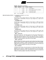
Table 30.
DDBn Effects on Port B Pins
DDBn
PORTBn
I/O
Pull-up
Comment
0
0
Input
No
Tri-state (high-Z)
0
1
Input
Yes
PBn will source current if ext. pulled low
1
0
Output
No
Push-pull Zero Output
1
1
Output
No
Push-pull One Output


