6
ATmega103(L)
0945G–09/01
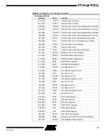
TOSC1
Input to the inverting Timer/Counter oscillator amplifier.
TOSC2
Output from the inverting Timer/Counter oscillator amplifier.
WR
External SRAM write strobe
RD
External SRAM read strobe
ALE
ALE is the Address Latch Enable used when the External Memory is enabled. The ALE
strobe is used to latch the low-order address (8 bits) into an address latch during the first
access cycle, and the AD0-7 pins are used for data during the second access cycle.
AVCC
Supply voltage for Port F, including ADC. The pin must be connected to VCC when not
used for the ADC. See “ADC Noise Canceling Techniques” on page 77 for details when
using the ADC.
AREF
AREF is the analog reference input for the ADC converter. For ADC operations, a volt-
age in the range AGND to AVCC must be applied to this pin.
AGND
If the board has a separate analog ground plane, this pin should be connected to this
ground plane. Otherwise, connect to GND.
PEN
PEN is a programming enable pin for the serial programming mode. By holding this pin
low during a power-on reset, the device will enter the serial programming mode. PEN
has no function during normal operation.
Clock Options
Crystal Oscillator
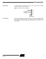
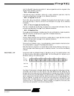
XTAL1 and XTAL2 are input and output, respectively, of an inverting amplifier, which
can be configured for use as an on-chip oscillator, as shown in Figure 2. Either a quartz
crystal or a ceramic resonator may be used.
Figure 2.
Oscillator Connections
Note:
When using the MCU oscillator as a clock for an external device, an HC buffer should be
connected as indicated in the figure.
XTAL2
XTAL1
GND
C2
C1
MAX 1 HC BUFFER
HC

