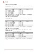
32
Interfaces
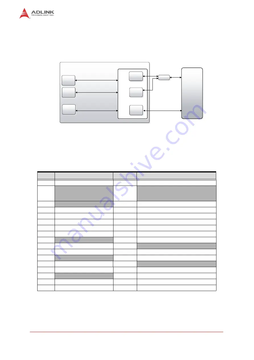
3.24 LVDS Interface (CN66)
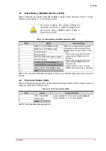
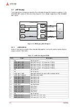
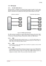
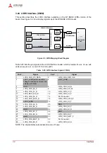
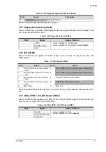
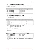
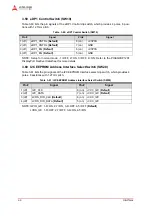
This section describes the LVDS interface available on the Q7-BASE LVDS version of the
board. See Figure 3-3 for a display signal map of the Q7-BASE LVDS model.
Figure 3-3: LVDS Mapping Block Diagram
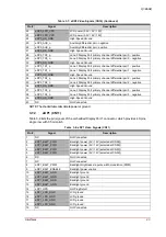
Table 3-25 lists the pin signals of the LVDS Interface header, which provides 3
4 pins, 2 rows, with
odd/even sequence (1, 2) and 0.079
" (2mm) pitch.
NOTE: The shaded table cells denote Ground or Power.
Table 3-25: LVDS Interface Signals (CN66)
Pin #
Signal
Pin #
Signal
1
LVDS_CON_DC_DATA
2
LVDS_CON_DDC_CLK
3
+VCC_LVDS (switched LVDS
voltage controlled by chipset and
selected at CN62)
4
+VCC_LVDS
5
GND
6
LVDS_CON_A0_N
7
LVDS_CON_A0_P
8
LVDS_PWR_EN_NI
9
LVDS_CON_A1_N
10
LVDS_CON_A1_P
11
LVDS_BKLT_EN_NI
12
LVDS_CON_A2_P
13
LVDS_CON_A2_N
14
Not Connected
15
LVDS_CON_ACLK_N
16
LVDS_CON_ACLK_P
17
+VCC_LVDS
18
LVDS_CON_A3_P
19
LVDS_CON_A3_N
20
GND
21
LVDS_CON_B0_N
22
LVDS_CON_B0_P
23
GND
24
LVDS_CON_B1_N
25
LVDS_CON_B1_P
26
GND
27
LVDS_CON_B2_N
28
LVDS_CON_B2_P
29
GND
30
LVDS_CON_BKLT_P
31
LVDS_CON_BKLT_N
32
Not Connected
33
LVDS_CON_B3_P
34
LVDS_CON_B3_N
Con
n
e
ct
o
r (
M
X
M
2)
Intel®
Apollo Lake
SoC
HDMI/DP
3840x2160@30Hz
LVDS
Primary
Channel
LVDS
Secondary
Channel
HDMI/DP
NXP
DDI
DDI
Q7-BASE (LVDS op
Ɵ
on)
BLK
LVDS (18/24bit)
Pin header
2x 17
Pin header
2x 4
BLK
HDMI
or
DP
Single/Dual Channel
BLK
HDMI/DP
1920x1200@60Hz