3
© February 2007 TOSHIBA TEC CORPORATION All rights reserved
e-STUDIO167/207/237
COPY PROCESS
3 - 1
3.
COPY PROCESS
3.1
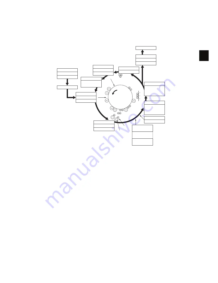
General Description of Copying Process
Fig. 3-1
(1)
Charging: Applies negative charge on the
surface of the photoconductive drum.
(7)
Separation: Separates paper with the toner
image from the photoconductive drum.
#
#
(2)
Data reading: The images on the original
are converted into electrical signals.
(8)
Fusing: Fuses the toner image onto the
paper by applying heat and pressure.
#
#
(3)
Data writing: The electrical signals are con-
verted into light signal (laser emission)
which exposes the surface of the photo-
conductive drum.
(9)
Cleaning: Scrapes off the residual toner
from the drum.
#
#
(4)
Development: Negatively-charged toner
adheres to the photoconductive drum and
forms visible image.
(10)
Discharging: Eliminates the residual nega-
tive charge from the surface of the photo-
conductive drum.
#
(5)
Transfer bias: Improves transfer efficiency.
#
(6)
Transfer: Transfers the visible toner image
on the photoconductive drum onto paper.
#
Data reading(scanning)
CIS
600 dpi,7084 pixel
Image processing
Discharging
Discharge LED (red)
Wavelength 660nm x10pcs
(10)
(8)
(7)
(6)
(5)
(9)
(2)
(1)
(3)
(4)
Data writing
Semiconductive laser
Pw=4.0 nJ/mm
2
Charging
e-STUDIO167/207:-448V
e-STUDIO237 :-454V
(grid voltage)
Development
Magnetic roller
Bias -AC
Toner
Carrier
Cleaning
Blade method
Bypass feeding
(100 sheets)
Drawer feeding
(250 sheets)
PFU
(250 sheets)
Transfer
H
340 µADC
C
369 µADC
L
282 µADC
Separation
H -107 µADC
Paper exit
Fusing
Lamp heating method
564W x2
Transfer bias
DC +565V
L -70 µADC
C -107 µADC
Содержание E-Studio167
Страница 8: ...e STUDIO167 207 237 February 2007 TOSHIBA TEC CORPORATION All rights reserved CONTENTS 4 ...
Страница 54: ...e STUDIO167 207 237 February 2007 TOSHIBA TEC CORPORATION All rights reserved OUTLINE OF THE MACHINE 2 38 ...
Страница 68: ...e STUDIO167 207 237 February 2007 TOSHIBA TEC CORPORATION All rights reserved COPY PROCESS 3 14 ...
Страница 92: ...e STUDIO167 207 237 February 2007 TOSHIBA TEC CORPORATION All rights reserved CONTROL PANEL 5 10 ...
Страница 132: ...e STUDIO167 207 237 February 2007 TOSHIBA TEC CORPORATION All rights reserved LASER OPTICAL UNIT 8 8 ...
Страница 142: ...e STUDIO167 207 237 February 2007 TOSHIBA TEC CORPORATION All rights reserved DRIVE UNIT 9 10 ...
Страница 192: ...e STUDIO167 207 237 February 2007 TOSHIBA TEC CORPORATION All rights reserved DRUM RELATED SECTION 11 22 ...
Страница 214: ...e STUDIO167 207 237 February 2007 TOSHIBA TEC CORPORATION All rights reserved DEVELOPMENT SYSTEM 12 22 ...
Страница 260: ...e STUDIO167 207 237 February 2007 TOSHIBA TEC CORPORATION All rights reserved POWER SUPPLY UNIT 15 8 ...
Страница 264: ...e STUDIO167 207 237 February 2007 TOSHIBA TEC CORPORATION All rights reserved PC BOARDS 16 4 8 PWA F ADU Fig 16 8 ...
Страница 265: ......
Страница 266: ......


