Application Note P4097
© TeraTron GmbH
Page 4 of 21
V1.1, 07.06.01
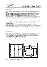
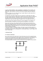
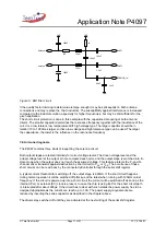
L
txp
and L
ant
form the transformer, they are coupled by a mutual inductor which is not drawn. The
quality factor of both resonance circuits is determined by the resistors R
txp
, R
ltxp
and R
ant
which
represent the copper resistances, the eddy current losses and supply current of the transponder
circuit.
To achieve a large current in the antenna with a given supply voltage and a limited quality factor a
bridge configuration for the driver is chosen.
The transponder incorporates a parallel resonance circuit because a high voltage at low supply
currents is needed, whereas the reader/exciter is realized using a series resonance circuit because a
low supply voltage should cause a high antenna current. The series resonance circuit has a low
impedance at the resonance frequency and allows high driving currents (and therefore strong
magnetic fields) using a low driving voltage, the opposite is true for the parallel resonance circuit.
The voltage change at the reader/exciter antenna can be demodulated as it is modulated by the
different damping of the transponder circuit (as long as the coupling factor is not too small).
If the resonance frequency of the transponder and the resonance frequency of the antenna are
different the coupling factor between both coils becomes complex. This means that the modulated
signal is phase shifted against the carrier signal. If this phase shift reaches 90° the signal can not be
demodulated with a simple peak detector any more as the carrier is being pure phase modulated
without any amplitude modulation.
To avoid this so called “zero modulation problem” and therefore increase the allowed tolerances of
components the P4097 is able to detect amplitude- and phase modulation. The demodulation is done
by a sampling principle where the sampling phase can be switched between 0° and 90° relative to the
antenna driving voltage.
3. Hardware Design
3.1 Thermal considerations
Due to resistive losses in the antenna driver circuit and the supply current for the integrated analog
circuitry the chip is generating heat during operation which is increasing the junction temperature. As
mentioned in the data sheet this junction temperature shall not exceed 110°C to guarantee the
electrical characteristics of the chip and therefore the functionality of the whole circuit.
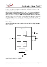
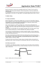
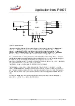
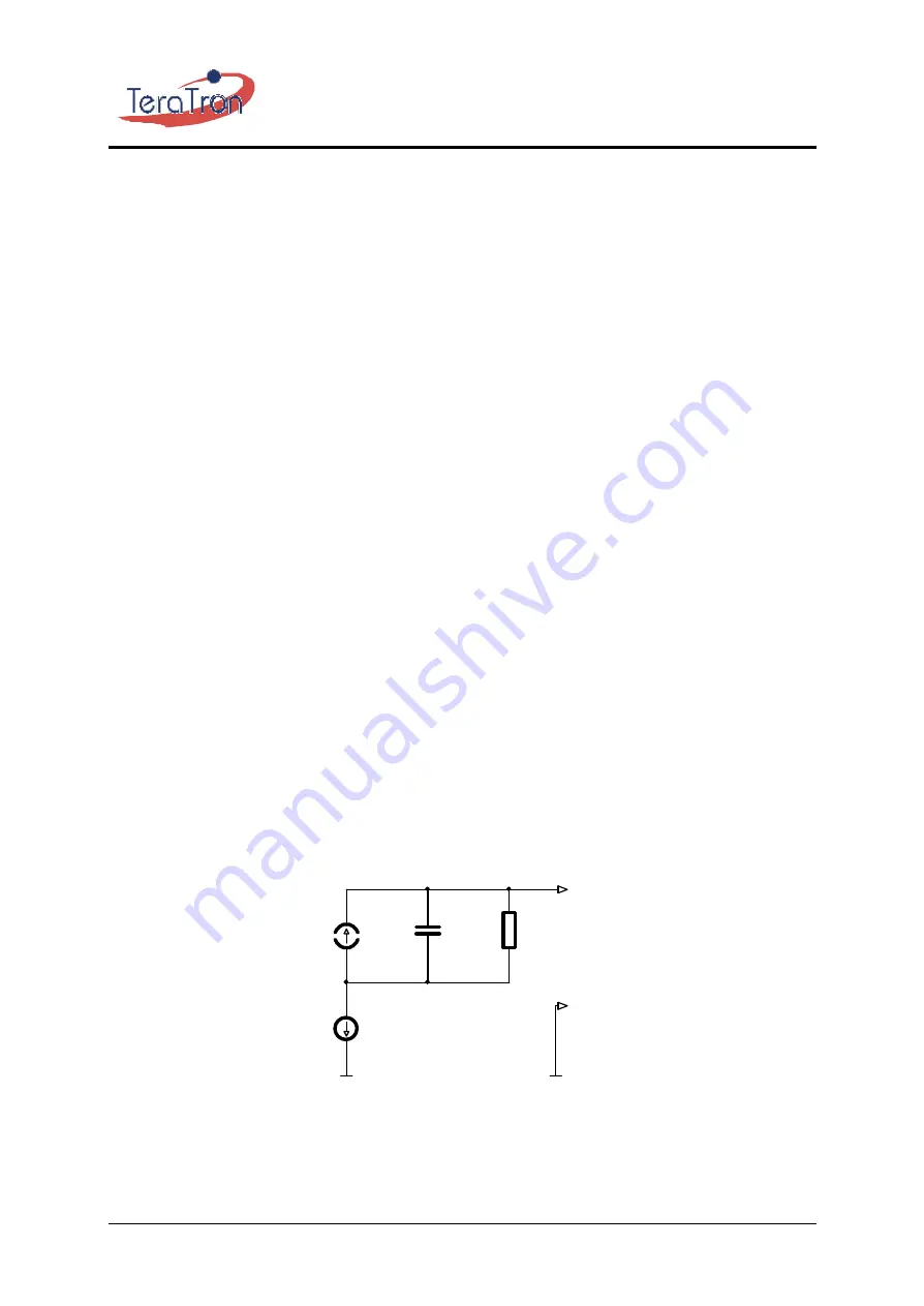
The following simplified schematic is useful for calculating the junction temperature during operation.
Ta
Rtja
Tj(+)
GND
Pv
Tj(-)
Ctja
GND
Figure 2.: Equivalent schematic for thermal calculations

