Application Note P4097
© TeraTron GmbH
Page 6 of 21
V1.1, 07.06.01
themselves are equipped with a “break-before-make” circuitry and do not draw a cross current. The
capacitor is needed to suppress EMI.
The antenna is deenergized by diodes connected to V
SS
and V
DD
, the push-pull antenna drivers are in
tri-state if switched off. Therefore the voltage shortly after the driver has being switched off reaches
about V
DD
+ 1V and V
SS
– 1V for a few 125kHz cycles depending on the quality factor of the antenna.
Take care that the OUT pin, connected buffers or similar, must not switch high currents. Together with
a weak power supply this can form a resonant loop. The switched current modulates the supply
voltage which can be seen as amplitude modulation on the DEMOD_IN which is demodulated through
the chip to the OUT signal.
3.3 Filter design
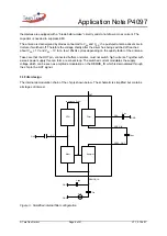
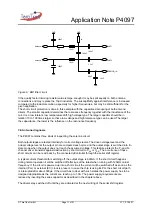
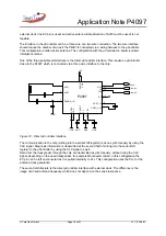
The internal demodulation chain of the chip is shown below. The schematic is simplified but contains
all stages of interest.
OUT
CDEC_OUT
Vin
Cdc
GND
CF
GND
GND
Filter
GND
Mixer
DEMOD_IN
VCO
CDEC_IN
CDC
Cgnd
to Antenna Driver
Sampler
Cin
Cdec
Figure 3.: Simplified internal filter configuration

