Application Note P4097
© TeraTron GmbH
Page 5 of 21
V1.1, 07.06.01
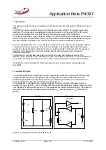
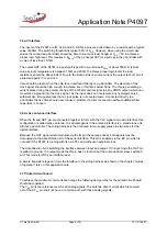
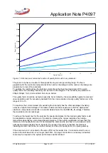
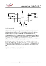
In this circuit Ta is the ambient temperature, T
j
is the junction temperature (to be calculated) and C
tja
and R
tja
are the thermal capacitance and resistance as given in the datasheet for the chip soldered on
a 2 layer 1.5mm FR4 board with 35µm copper using a standard SO-16 footprint.
The current source P
v
represents the power which has to be dissipated. It is calculated as follows:
AD
Ant
DDon
DD
V
R
I
I
V
P
⋅
+
⋅
=
2
2
ˆ
,
with V
SS
= 0V
with the antenna current determined by:
loop
DD
Ant
R
V
I
⋅
Π
=
4
ˆ
and the loop resistance given with:
AD
Ant
loop
R
R
R
+
=
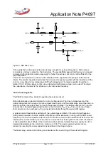
Putting all above into an electric circuit simulation (or using the appropriate formulas) the junction
temperature even for pulsed operation at the antenna driver current limit can be calculated. The
surrounding circuit, ambient temperature and the duty cycle should be chosen that by no means a
junction temperature of 110°C is exceeded.
3.2 Power Supply
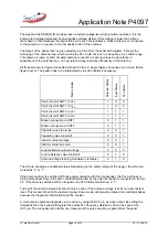
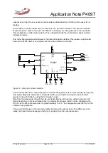
The circuit has to be supplied with a regulated voltage in the range given in the datasheet. The
consumed current in active mode can be calculated with:
DDon
Ant
Sup
I
I
I
+
⋅
Π
=
ˆ
2
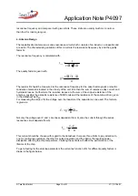
The power supply should be able to supply this current without voltage fluctuations and ripple. This
ripple on V
DD
will be seen as modulation on the DEMOD_IN pin and can especially in the frequency
range of transponder communication not be distinguished from data send by the transponder. To get a
feeling for the supply voltage rejection of the circuit, as there will be always a certain amount of ripple
because of non perfect components, for a typical configuration the drop of the DEMOD_IN peak
voltage is 50mV if the V
DD
is decreased by 62.5mV. The transponder itself is modulating by a few tens
of mV. It can be seen that an insufficient power supply can easily cause malfunction or at least a
reduction in functionally and read/write range.
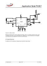
As a good design practice the power supply capacitor should be split and a 10µF capacitor with a low
ESR together with a ceramic 100nF capacitor are being placed in direct vicinity of the chip. A ripple
voltage smaller than 5mV
SS
in the frequency range between 100Hz up to 10kHz should be achieved
for best results. For higher or lower frequencies the susceptibility is reduced due to the receive band
pass filter.
The 10µF is needed to suppress the sourcing of antenna current into V
DD
in case the antenna driver is
being modulated. Too little capacitance together with a low power circuit will result in a lifted V
DD
in the
moment when the antenna is switched off as the voltage regulator can usually not sink current.
The 100nF ceramic capacitor supplies the output stage with the short current peaks which are drawn
by the pre-driver stage when the output level changes between V
SS
and V
DD
. The output transistors

