Application Note P4097
© TeraTron GmbH
Page 19 of 21
V1.1, 07.06.01
GND
to µC
GND
from µC
GND
P4097
1
10
2
3
5
4
6
7
8
9
13
12
11
14
15
16
VSS
CLK
ANT1
DVDD
DVSS
ANT2
VDD
DEMOD_IN
CDEC_OUT
CDEC_IN
CAGND
OUT
IN
CF
CDC
EC
GND
from µC
5V
from µC
GND
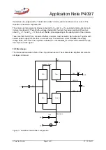
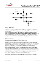
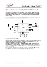
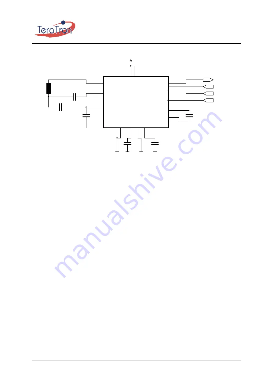
Figure 13.: External clock
The division factor between EC pin and antenna driver is 32 and fixed. Therefore the external clock
has to have a 4MHz frequency when using a 125kHz transponder. 125kHz is then the carrier
frequency for the data and energy transmission. Care should be taken when routing this high
frequency signal from the source to the chip. To avoid electromagnetic emission the clock source
should be located close to the P4097. The slew rate should not be higher than necessary.
If a crystal is shared between the µController and the P4097, the additional capacitance of the trace
and the input should not be disregarded to achieve a stable start up. The input capacitace is given in
the datasheet. Capacitive coupling in of high frequency signals must be avoided.
Any jitter on this signal reduces the system performance, µController using a PLL for clock generation
have to be checked carefully on their clock signal stability.
The CF pin is connected to ground as the internal VCO is not needed.
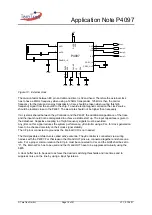
The third possible architecture is called active antenna. The µController is connected via a wiring
harness with the P4097. For that reason the IN and OUT pins are connected together and share one
wire. For a proper communication the EC pin must be connected to V
SS
and the bit#4 shall be set to
“0”. The internal PLL has to be used and the IN and OUT have to be suppressed mutually using the
bit#3.
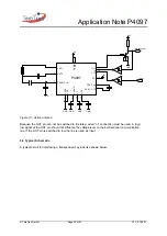
A clock buffer has to be used to achieve the desired switching thresholds and rise times and to
suppress noise on the line by using a input hysteresis.

