Application Note P4097
© TeraTron GmbH
Page 20 of 21
V1.1, 07.06.01
GND
5V
GND
GND
Input
Bidirectional
GND
GND
P4097
1
10
2
3
5
4
6
7
8
9
13
12
11
14
15
16
VSS
CLK
ANT1
DVDD
DVSS
ANT2
VDD
DEMOD_IN
CDEC_OUT
CDEC_IN
CAGND
OUT
IN
CF
CDC
EC
GND
5V
12V
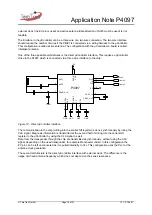
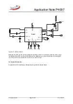
Figure 14.: Active antenna
Because the OUT pin can not be switched to tri-state a wired “or” connection must be used. A logic
low signal at the OUT pin should not influence the voltage level on the bi-directional communication
line. If the OUT pin is switched to low the line is used as input.
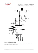
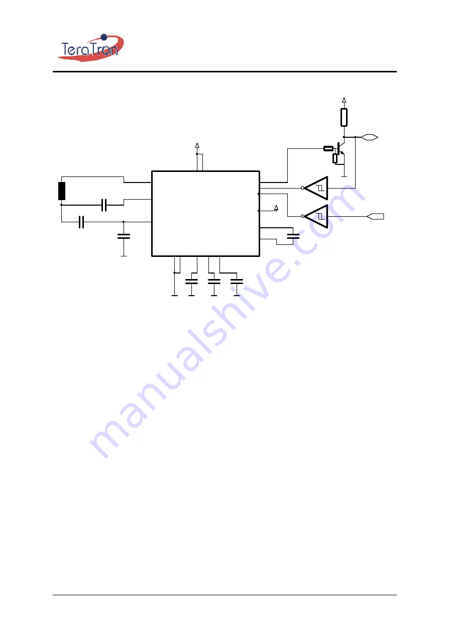
5.4 Typical Schematic
A typical circuit for interfacing a transponder may look like shown below.

