72
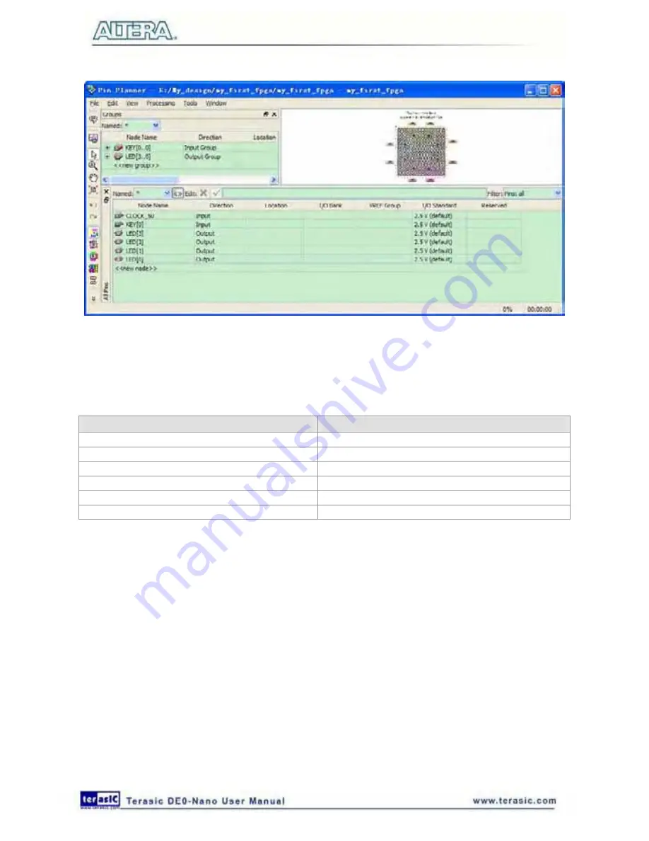
Figure 6-41 Pin Planner Example
2. In the Location column next to each of the six node names, add the coordinates (pin numbers)
as shown in
Table 6-1
for the actual values to use with your DE0-Nano board.
Table 6-1 Pin Information Setting
Pin Name
FPGA Pin Location
KEY[0]
J15
LED[3]
A11
LED[2]
B13
LED [1]
A13
LED [0]
A15
CLOCK_50
R8
Double-click in the Location column for any of the six pins to open a drop-down list and type the
location shown in the table. Alternatively, you can select the pin from a drop-down list. For example,
if you type
F1
and press the
Enter
key, the Quartus II software fills in the full PIN_F1 location
name for you. The software also keeps track of corresponding FPGA data such as the I/O bank and
VREF Group. Each bank has a distinct color, which corresponds to the top-view wire bond drawing
in the upper right window, as shown in
Figure 6-42
.
Содержание De0-Nano
Страница 1: ...1 ...
Страница 4: ...4 9 3 Revision History 155 9 4 Copyright Statement 155 ...
Страница 44: ...44 Figure 6 5 Browse to find the location Figure 6 6 There is no need to test the driver ...
Страница 90: ...90 Figure 7 14 Add NIOS II Processor ...
Страница 91: ...91 Figure 7 15 Nios II Processor 9 Click Finish to return to main window as shown in Figure 7 16 ...
Страница 93: ...93 Figure 7 17 Rename the CPU 1 Figure 7 18 Rename the CPU 2 ...
Страница 98: ...98 Figure 7 23 Add On Chip Memory ...
Страница 100: ...100 Figure 7 25 Update Total memory size ...
Страница 102: ...102 Figure 7 28 Update CPU settings ...
Страница 104: ...104 Figure 7 30 Add PIO ...
Страница 106: ...106 Figure 7 32 PIO 21 Rename pio_0 to pio_led as shown in Figure 7 33 Figure 7 33 Rename PIO ...
Страница 113: ...113 Figure 7 43 Input verilog Text Figure 7 44 Open DE0_NANO_SOPC v ...
Страница 146: ...146 Figure 8 16 Display Progress and Result Information for the SDRAM Demonstration ...
Страница 150: ...150 Figure 9 3 Select Devices Page ...
Страница 151: ...151 Figure 9 4 Convert Programming Files Page ...


