138
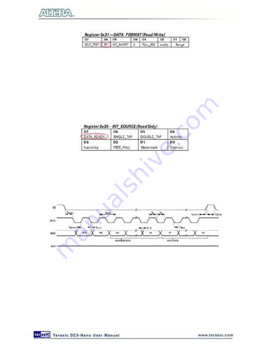
Figure 8-8 DATA_FORMAT Register
The data format is configured as 10 bits, right-justify, +/- 2g mode. The output data rate is
configured as 400 HZ. The X/Y/Z value is read using polling mode. Before reading X/Y/Z, the
master needs to make sure data is ready by reading the register 0x30-INT_SOURCE, as shown
below
Figure 8-9
, and checking the DATA_READY bit. In the demo, multiple-byte read of six
bytes X/Y/Z, register from 0x32 to 0x37, is performed to prevent a change in data between reads of
sequential register. Note, the output data is twos complement with DATAx0 as the least significant
byte and DATAx1 as the most significant byte, where x represent X, Y, or Z.
Figure 8-9 Register 0x30
The SPI timing scheme follows clock polarity (CPOL)=1 and clock phase (CPHA)=1. (CPOL)=1
means the clock is high in idle. (CPHA)=1 means data is captured on clock’s rising edge and data is
propagated on a falling edge. The timing diagram of 3-wire SPI is shown below
Figure 8-10
:
Figure 8-10 3-wire SPI Timing Diagram
ADC Control
The Analog to Digital Conversion is controller through a 4-wire SPI interface with the timing dialog
given below
Figure 8-11
. Note, the DIN signal is used to specify the channel (IN0~IN7) for the
next data conversion. The DOUT signal is used to read the data conversion result whose channel is
specified in previous transaction. The first conversion result after power-up will be on IN0. The
output format of conversion result is straight binary.
Содержание De0-Nano
Страница 1: ...1 ...
Страница 4: ...4 9 3 Revision History 155 9 4 Copyright Statement 155 ...
Страница 44: ...44 Figure 6 5 Browse to find the location Figure 6 6 There is no need to test the driver ...
Страница 90: ...90 Figure 7 14 Add NIOS II Processor ...
Страница 91: ...91 Figure 7 15 Nios II Processor 9 Click Finish to return to main window as shown in Figure 7 16 ...
Страница 93: ...93 Figure 7 17 Rename the CPU 1 Figure 7 18 Rename the CPU 2 ...
Страница 98: ...98 Figure 7 23 Add On Chip Memory ...
Страница 100: ...100 Figure 7 25 Update Total memory size ...
Страница 102: ...102 Figure 7 28 Update CPU settings ...
Страница 104: ...104 Figure 7 30 Add PIO ...
Страница 106: ...106 Figure 7 32 PIO 21 Rename pio_0 to pio_led as shown in Figure 7 33 Figure 7 33 Rename PIO ...
Страница 113: ...113 Figure 7 43 Input verilog Text Figure 7 44 Open DE0_NANO_SOPC v ...
Страница 146: ...146 Figure 8 16 Display Progress and Result Information for the SDRAM Demonstration ...
Страница 150: ...150 Figure 9 3 Select Devices Page ...
Страница 151: ...151 Figure 9 4 Convert Programming Files Page ...


