63
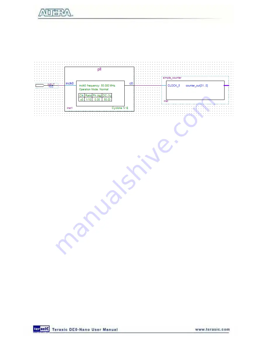
4. Place the new pin onto the BDF so that it is touching the input to the pll symbol.
5. Use the mouse to click and drag the new input pin to the left; notice that the ports remain
connected as shown in
Figure 6-29
.
Figure 6-29 Connecting the PLL symbol and Input port
6. Change the pin name by double-clicking pin_name and typing CLOCK_50 (see
Figure 6-30
).
This name correlates to the oscillator clock that is connected to the FPGA.
Adding an Output bus to the Schematic
The following steps describe how to add an output bus to the schematic.
1. Using the Orthogonal Bus tool, draw a bus line connected on one side to the simple_counter
output port, and leave the other end unconnected at about 4 to 8 grid spaces to the right of the
simple_counter.
Содержание De0-Nano
Страница 1: ...1 ...
Страница 4: ...4 9 3 Revision History 155 9 4 Copyright Statement 155 ...
Страница 44: ...44 Figure 6 5 Browse to find the location Figure 6 6 There is no need to test the driver ...
Страница 90: ...90 Figure 7 14 Add NIOS II Processor ...
Страница 91: ...91 Figure 7 15 Nios II Processor 9 Click Finish to return to main window as shown in Figure 7 16 ...
Страница 93: ...93 Figure 7 17 Rename the CPU 1 Figure 7 18 Rename the CPU 2 ...
Страница 98: ...98 Figure 7 23 Add On Chip Memory ...
Страница 100: ...100 Figure 7 25 Update Total memory size ...
Страница 102: ...102 Figure 7 28 Update CPU settings ...
Страница 104: ...104 Figure 7 30 Add PIO ...
Страница 106: ...106 Figure 7 32 PIO 21 Rename pio_0 to pio_led as shown in Figure 7 33 Figure 7 33 Rename PIO ...
Страница 113: ...113 Figure 7 43 Input verilog Text Figure 7 44 Open DE0_NANO_SOPC v ...
Страница 146: ...146 Figure 8 16 Display Progress and Result Information for the SDRAM Demonstration ...
Страница 150: ...150 Figure 9 3 Select Devices Page ...
Страница 151: ...151 Figure 9 4 Convert Programming Files Page ...


