267
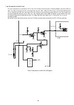
Main Switching Circuit
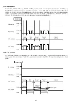
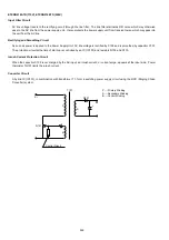
In the above circuit, when the main switching transistor, Q101, is turned On, input voltage, Ei, is supplied to the primary winding
of transformer T101. However, no current will flow through diode D201 of the secondary side, due to reverse polarity of the
secondary winding causing no current flow within T1. But the transformer charges with energy. When Q101 is turned Off, the
supply voltage to the primary winding shuts off and the windings of T101 change polarity, allowing D201 to conduct, releasing
the energy accumulated in T101 to the circuit. When the energy is discharged through D201, Q101 turns on, once again
reversing the polarity on T101 windings, creating a self-oscillation circuit.
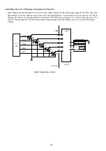
In the actual circuit, the fixed output voltages are obtained by changing the winding ratio of transformer T101. In this converter
circuit, the output voltages are stabilized by controlling the duty cycle of the ON and OFF timing of the transistor. In this power
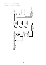
supply, the bias winding is built into the transformer. The power supply has four outputs, +24 VDC, -12 VDC, +5 VP and +5 VDC.
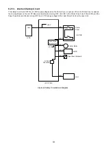
The +24 VDC output is protected by the Error Detection Circuit, and the +5 VP and -12 VDC outputs are protected by the
circuitry inside of the voltage regulator IC, +5 VDC is protected by ZD251.
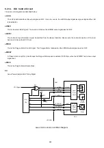
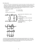
he value of output voltage is
o=d/(1-d)*Ei
=Ton/Ts
quivalent circuit model for the RCC.
Ton : On time of Q101
In the equivalent circuit ; When SW is on, current
flows
SW L
When SW is off, current flows
L D RL
The value of inductance increase current between
on period. (d*Ts)
IL=Ei/L*d*Ts . . . . . . . . . . . . . . . . . .(1)
The value of inductance decrease current between
off period. ((1-d)*Ts) . . . . . . . . . . . . . . . .(2)
From equation (1) and (2),
Eo=d/(1-d)*Ei
Ts : Period of oscillation
VL
VL
L
C
T101
D(D201)
Eo
Eo
Ts
dTs
RL
Ei
SW
(Q101)
T
IL
Ei
(1-d)Ts
dTs
Содержание Panafax DX-2000
Страница 2: ......
Страница 27: ...27 9 1 Screw 19 10 Release two Latch Hooks 11 Remove the SNS Assembly 121 9 10 11 ...
Страница 49: ...49 2 15 Screw Identification Template ...
Страница 56: ...56 3 7 2 Printer Circuit 429 650 622 744 607 665 555 506 432 408 405 433 502 610 610 610 621 507 507 639 ...
Страница 57: ...57 3 7 3 Option Cassette Circuit 555 748 728 744 928 953 730 731 731 952 944 930 931 931 ...
Страница 58: ...58 3 7 4 LAN Control Circuit 522 CN50 1102 1104 1101 N C N C RD N C N C RD TD TD ...
Страница 59: ...59 3 7 5 Page Description Language Printer Interface Kit ...
Страница 287: ...314 B Supplies Order No Picture Description DZHT000004 Verification Stamp UG 3313 Toner Cartridge ...

