background image

CDV Construction Manual – Issue 3 

Page 3 


List of Figures 


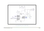
Figure 1 Microcontroller and power supply schematic ................................................................................... 8


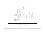
Figure 2 Si5351A Clock generator schematic ....................................................................................................... 9


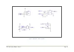
Figure 3 Display and controls schematic ............................................................................................................. 10


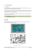
Figure 4 Component overlay .................................................................................................................................... 12


Figure 5 OLED mounting ............................................................................................................................................ 15


Figure 6 CDV panel cutting ........................................................................................................................................ 17


Figure 7 CDV used in a superhet rig ...................................................................................................................... 25


Figure 8 Add-on board options ................................................................................................................................ 26


Figure 9 Add-on board schematic ........................................................................................................................... 27


Figure 10 Add-on board PCB overlay .................................................................................................................... 27


Figure 11 Attenuator filter board fitted to the CDV ........................................................................................ 30


Change History 

Date 

Issue 

Comments 

30-Jan-2017 

First release 

10-Jan-2020 

Added BFO fixed output feature. Added user programmable steps. 

Improved frequency accuracy. Minor text changes. 

1-Oct-2020 

Rev. B PCB. 2 pin JST connector reversed, alternative 4 pin connector 

wire colours. 


Содержание CDV

Страница 1: ...CDV Construction Manual Issue 3 Page 1 CDV COMPACT DIGITAL VFO CONSTRUCTION MANUAL ...

Страница 2: ...ng to a panel 17 9 Set up 18 9 1 General 18 9 2 Procedure 18 9 3 Understanding Menu options 18 9 4 Menu Option Ranges 21 10 Operation 22 10 1 Operating Display 22 10 2 Tuning 22 10 3 Step selection 22 10 4 Scan mode 23 10 5 RIT 23 10 6 VFO Frequency calibration 24 10 7 Voltage display calibration 24 11 Using the CDV with a superhet rig 25 12 Optional Attenuator Low pass Filter Board 26 12 1 Schema...

Страница 3: ... 17 Figure 7 CDV used in a superhet rig 25 Figure 8 Add on board options 26 Figure 9 Add on board schematic 27 Figure 10 Add on board PCB overlay 27 Figure 11 Attenuator filter board fitted to the CDV 30 Change History Date Issue Comments 30 Jan 2017 1 First release 10 Jan 2020 2 Added BFO fixed output feature Added user programmable steps Improved frequency accuracy Minor text changes 1 Oct 2020 ...

Страница 4: ...eps BFO fixed output feature provides a replacement for a crystal in superhet rigs Simple and flexible configuration through on screen menus Clear and bright low current OLED display Very small overall size Simple control via a rotary encoder and two small pushbuttons Low power consumption Wide frequency range IF offset function Scanning function Receiver incremental Tuning RIT RX TX indication US...

Страница 5: ... VFO IF NONE 9 Receiver incremental Tuning RIT range no limit 10 Programmable frequency steps Select from the range 1Hz 10Hz 100Hz 1KHz 5Khz 10KHz 25KHz and 100KHz 11 Operating supply voltage range 5 to 15V DC 12 Average operating current 35mA 13 TX RX and USB LSB logic inputs An input larger than 3 3V is logic high 14 Low power supply alarm 5 to 15V DC 15 Output impedance 50 Ohms 16 Output drive ...

Страница 6: ...900MHz The PLL outputs are directed by the matrix switch to the respective fractional divider where the PLL frequency is divided down to provide the desired output frequency The PLL and fractional dividers are controlled by a microcontroller via an I2C interface Through a combination of programmable PLL frequencies and fractional divider values the clock generator is capable of outputting frequenc...

Страница 7: ...ress button switch input on U1 pin 1 and is used for a number of functions as described later U1 incorporates pull up resistors for the encoder inputs so they are normally held high and capacitors C9 and C10 help limit encoder switch bounce The CDV uses a small 0 96 inch monochrome 128 x 64 pixel matrix OLED for display If characters were written unmodified to the matrix they would be small and di...

Страница 8: ...CDV Construction Manual Issue 3 Page 8 Figure 1 Microcontroller and power supply schematic ...

Страница 9: ...CDV Construction Manual Issue 3 Page 9 Figure 2 Si5351A Clock generator schematic ...

Страница 10: ...CDV Construction Manual Issue 3 Page 10 Figure 3 Display and controls schematic ...

Страница 11: ...or ceramic MLCC SMD 0603 C9 10nF Capacitor ceramic MLCC SMD 0603 C10 10nF Capacitor ceramic MLCC SMD 0603 C11 100nF Capacitor ceramic MLCC SMD 0603 C12 100nF Capacitor ceramic MLCC SMD 0603 R1 22K Resistor 1 SMD 0603 R2 22K Resistor 1 SMD 0603 R3 22K Resistor 1 SMD 0603 R4 1K Resistor 1 SMD 0603 R5 22K Resistor 1 SMD 0603 R6 22K Resistor 1 SMD 0603 R7 4 7K Resistor 1 SMD 0603 R8 4 7K Resistor 1 SM...

Страница 12: ...tions it refers to the side of the PCB where the SMD parts are installed The reverse side is referred to as the solder side To assist construction the PCB has a screen printed component overlay and a solder mask to help guard against solder bridges The components are static sensitive Use anti static measures when handling the PCB out of its protective bag 6 2 STEPS Step 1 PCB Remove the PCB from i...

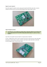
Страница 13: ...is to be used with an optional add on attenuator filter board decide if it is to be soldered directly to the PCB If being soldered directly the connector can be omitted Insert the two 2 pin JST connectors into the component side of the PCB For Rev A PCB the side of the connector with the cutout faces towards the top of the PCB If the PCB is Rev B the side of the connector with the cutout faces tow...

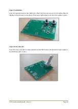
Страница 14: ...f the PCB It may be necessary to straighten the pins slightly so they fit easily Ensure they sit flat and at right angles to the PCB then solder in place Step 5 Rotary Encoder Insert the rotary encoder into the solder side of the PCB Ensure it sits flat and at right angles to the PCB then solder in place ...

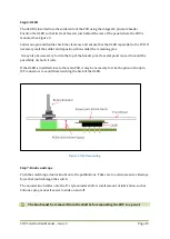
Страница 15: ...ry to trim the top of the header pins if a metal panel is used to avoid the possibility of short circuits If the OLED is installed close to the main PCB it may be necessary to trim the pins on the 2pin JST connectors to avoid them touching the back of the OLED Figure 5 OLED mounting Step 7 Knobs and caps Push the small long actuator knobs onto the pushbuttons Take care to avoid excessive sideways ...

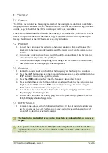
Страница 16: ...LS 1 Rotate the encoder knob and check that the frequency can be changed up and down 2 Press the SCAN button and check that Scan mode menu appears and select Exit with the STEP button to return to the operating screen 3 Press the STEP button and check that the frequency step can be changed 4 Press and hold the encoder button for a few seconds and check that the Set up screen is displayed Select FU...

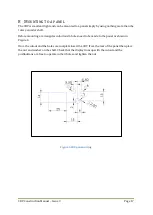
Страница 17: ...t Before mounting a rectangular cutout and 4 holes need to be made to the panel as shown in Figure 6 Once the cutout and the holes are complete insert the CDV from the rear of the panel then place the nut and washer on the shaft Check that the display lines up with the cutout and the pushbuttons are free to operate in their holes and tighten the nut Figure 6 CDV panel cutting ...

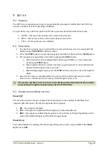
Страница 18: ...Menu options that have numerical values e g frequency are incremented and decremented using the rotary encoder c Menus displaying frequency use the STEP button to step the cursor through the digits 4 Once the last menu is completed the Set up procedure is exited and any new values stored in non volatile memory These are loaded again at power on The menus and their current values can be displayed a...

Страница 19: ... below the IF frequency and is most suitable when the TX frequency is below the IF frequency The VFO frequency is calculated in firmware using the following equations If TX frequency IF frequency then VFO frequency IF frequency TX frequency 80M example 6 5MHz 10MHz 3 5MHz If TX frequency IF frequency then VFO frequency TX frequency IF frequency 20M example 4MHz 14MHz 10MHz An IF Offset of NONE mea...

Страница 20: ...e as the transmit frequency Steps The option allows the selection of steps The step value is the amount the frequency is changed as the rotary encoder moves one position When this option is reached the current steps will be displayed If no changes are required simply press the SCAN button to go to the next option To change the steps do the following 1 Press the rotary encoder switch down briefly t...

Страница 21: ... be exact This option allows the displayed value to be trimmed to match the correct value SIDEBAND The CDV displays USB or LSB and calculates output frequencies depending on the state of the U L input wire This option allows the state to be reversed If the IF Offset option is set to NONE the USB LSB state will be ignored LO V Alarm This option flashes a low voltage message on the OLED when the sup...

Страница 22: ...crements the frequency while rotating counter clockwise decrements the frequency 10 3 STEP SELECTION Press the STEP button to cycle through the tuning frequency steps The step values must be set in Configuration when the CDV is first powered up When the rotary encoder is operated each indent will increment or decrement the frequency by the step value Receive Transmit indicator Step LSB USB indicat...

Страница 23: ...elected press the SCAN button again to start the scan 3 The scan frequency will be displayed along with a graphical bar at the bottom of the screen 4 The scan can be stopped in two ways a Press the SCAN button The tuning will revert to the initial tuned frequency before scan mode was started b Press the STEP button The tuning will be set to the frequency where scan mode was stopped If the scan mod...

Страница 24: ... remaining screens until Set up is exited 10 7 VOLTAGE DISPLAY CALIBRATION 1 Measure the power supply voltage and compare this to the voltage displayed on the OLED Note the difference a If the power supply voltage is less than the displayed voltage the difference needs to be subtracted in the Volts Calibrate screen b If the power supply voltage is greater than the displayed voltage the difference ...

Страница 25: ... sidebands Figure 7 shows the CDV used in a single conversion superhet transmitter for 40M Note how the Fixed outputs match the IF low and IF high skirt frequencies and that they change frequency automatically when the sideband is swapped Also note how the firmware automatically adjusts the VFO frequency when the sideband is swapped so that the transmit frequency does not shift Figure 7 CDV used i...

Страница 26: ... can be ordered in any attenuator filter combination Attenuator dB 50 ohms Low pass filter MHz 6dB 10MHz 12dB 20MHz 30MHz 40MHz Figure 8 Add on board options The low pass filter frequency shown in Figure 8 is the filter cut off frequency and it is important to understand how this relates to the VFO frequency and the output signal wave shape If the VFO frequency is near the cut off frequency the wa...

Страница 27: ...CDV Construction Manual Issue 3 Page 27 12 1 SCHEMATIC Figure 9 Add on board schematic 12 2 PCB OVERLAY Figure 10 Add on board PCB overlay ...

Страница 28: ...the solder and move gently with tweezers Once the component is located solder the other end using as little solder as possible Then go back to the first pad and apply a little more solder to ensure the joint is secure Inspect the job under a magnifier looking for solder bridges and dry joints Step 1 Resistors Locate and install the three SMD resistors R1 and R3 have the same value while R2 has a d...

Страница 29: ...irectly into the CDV PCB The OUT connector is a right angle JST 2 pin shrouded male header It is inserted into the component side 12 4 ATTACHING TO THE CDV There are two methods for attaching the board to the CDV 12 4 1 DIRECT In this method the board becomes a part of the CDV assembly Insert the 2 pins of the right angled header into the output holes on the CDV PCB Hold in place and solder into p...

Страница 30: ...CDV Construction Manual Issue 3 Page 30 Figure 11 Attenuator filter board fitted to the CDV ...

Отзывы: