CDV Construction Manual – Issue 3
Page 29
Step 3: Inductors
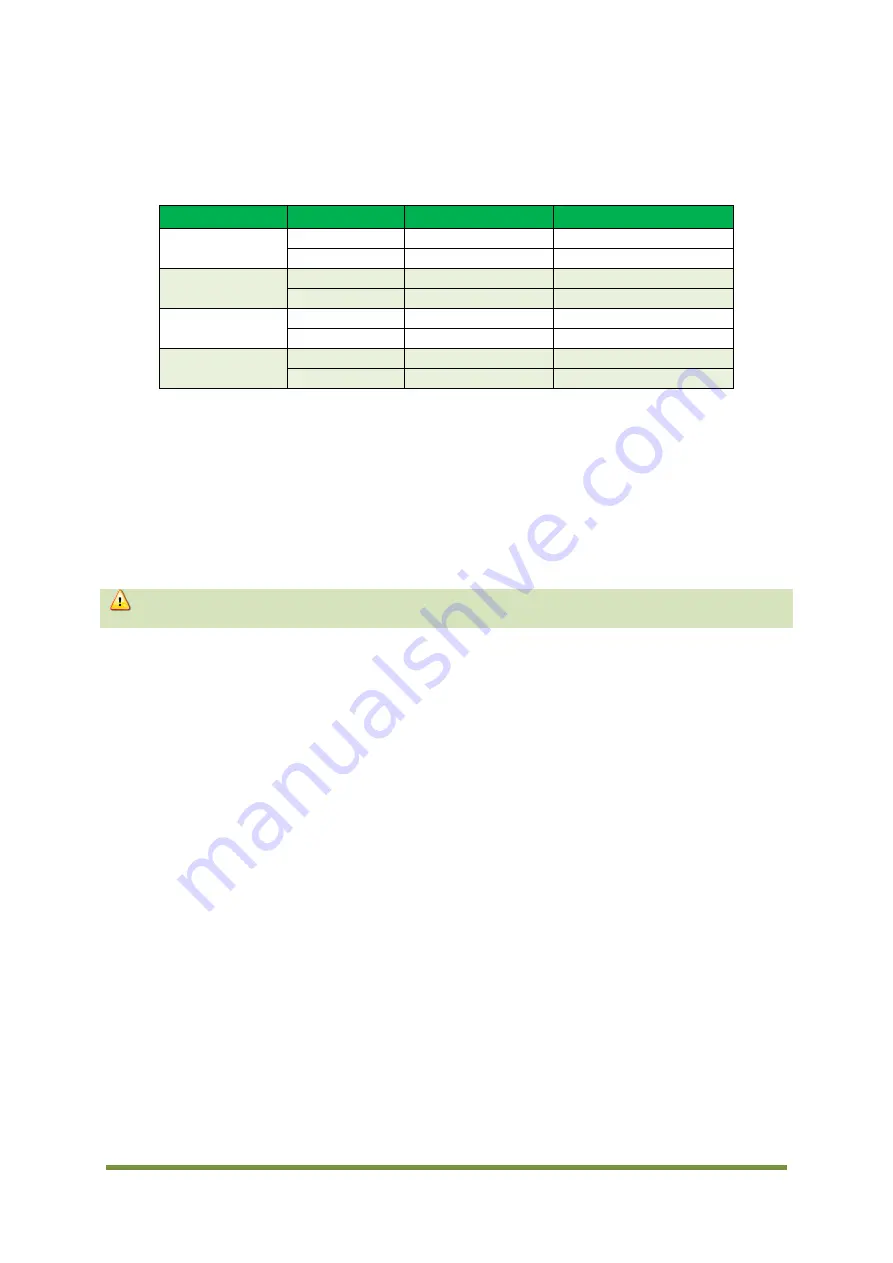
Locate and install the three SMD inductors. L1 and L3 have the same value, while L2 has a
different value. Use the table below to identify the correct values.
Filter
Inductor
Inductor label
Inductor Value
10MHz
L1, L3
1R0
1uH
L2
1R8
1.8uH
20MHz
L1, L3
R47
0.47uH
L2
R82
0.82uH
30MHz
L1, L3
R33
0.33uH
L2
R56
0.56uH
40MHz
L1, L3
R27
0.27uH
L2
R47
0.47uH
Step 4: Connectors
The IN connector is a 2 pin right angled male header. The end with shorter pins is soldered into
the PCB. The longer pins are soldered directly into the CDV PCB.
The OUT connector is a right angle JST 2 pin shrouded male header. It is inserted into the
component side.
12.4
A
TTACHING TO THE
CDV
There are two methods for attaching the board to the CDV.
12.4.1
D
IRECT
In this method the board becomes a part of the CDV assembly. Insert the 2 pins of the right
angled header into the output holes on the CDV PCB. Hold in place and solder into position.
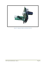
A directly mounted attenuator filter board is shown in Figure 11.
12.4.2
W
IRED
Here the board is located remotely from the CDV PCB and connected via wires. The supplied
connectors and cable may be used or omitted and discrete wiring used instead.
If the board is to be mounted externally and wired inline, then the connectors can
be omitted if desired.
Содержание CDV
Страница 1: ...CDV Construction Manual Issue 3 Page 1 CDV COMPACT DIGITAL VFO CONSTRUCTION MANUAL ...
Страница 8: ...CDV Construction Manual Issue 3 Page 8 Figure 1 Microcontroller and power supply schematic ...
Страница 9: ...CDV Construction Manual Issue 3 Page 9 Figure 2 Si5351A Clock generator schematic ...
Страница 10: ...CDV Construction Manual Issue 3 Page 10 Figure 3 Display and controls schematic ...
Страница 30: ...CDV Construction Manual Issue 3 Page 30 Figure 11 Attenuator filter board fitted to the CDV ...

