background image

Transmitter Description

User Manual

45

STEL-2176

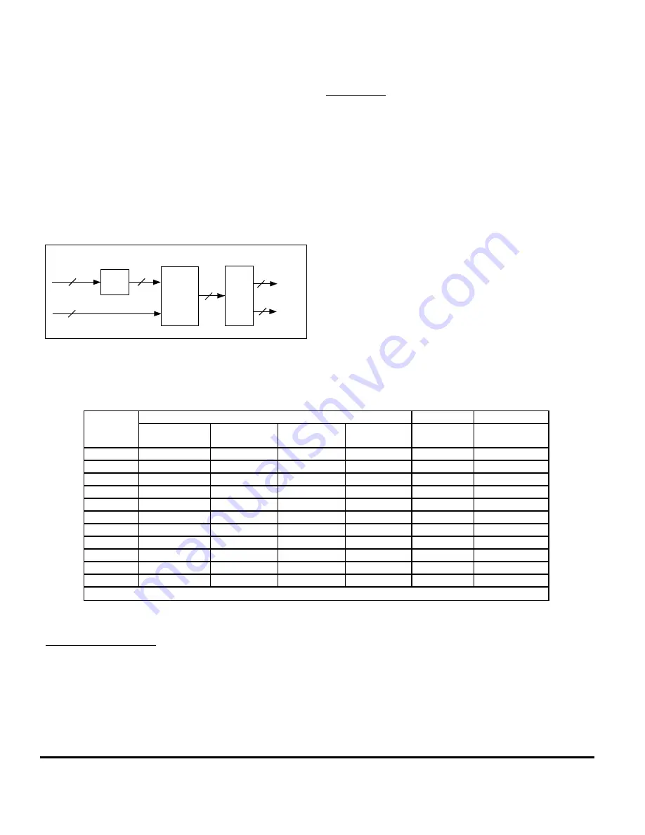
Symbol Mapper Block

The Symbol Mapper Block (Figure  28) maps the serial
data bits output by the Bit Encoder Block to symbols,
differentially encodes the symbols, and (in 16QAM)
maps the symbols to one of five constellations. The
Symbol Mapper Block functions are modulation
dependent. The modulation mode also defines the
number of bits per symbol. The Symbol Mapper Block
outputs 2 bits for each symbol to each of the two
Nyquist (FIR) Filters.

ENCODED
SERIAL DATA

I[1:0]

**

Q[1:0]

**

I[1:0]

*

Q[1:0]

*

I[1:0]

Q[1:0]

4

Bit

Mapper

Differential

Encoder

4

2

Symbol
Mapper

2

1

TXDIFFEN

1

WCP 53810.c-12/2/97

Figure 28.  Mapping Block Functional Diagram

Bit Mapper

The Bit Mapper receives serial data and maps the serial
data bits to output symbol bits (I

1

**

, I

0

**

, Q

1

**

, and Q

0

**

).

There are four output bits per symbol even in BPSK and
QPSK modes. In BPSK, all bits are set equal to each
other. In QPSK, each input symbol bit drives a pair of
output bits. The four symbol bits are routed to the
Differential Encoder in parallel.

For BPSK modulation, each bit (symbol = b

0

) of the

input serial data stream is mapped directly to I

1

**

, Q

1

**

,

I

0

**

, and Q

0

* *

 (i.e., I

1

**

= I

0

* *

= Q

1

**

= Q

0

**

= b

0

). Thus, bit

mapping has no affect on the respective value of the
symbolÕs four bits, as shown in Table 38.

For QPSK modulation, each pair of bits (a dibit) forms a
symbol (b

0

  b

1 )

. The QPSK dibit is mapped so that

I

1

**Ê

=ÊI

0

**

 and Q

1

** 

=


Q

0

**, 

as shown in Table 38.

For 16QAM, every four bits (a nibble) forms a symbol
(b

0

b

1

b

2

b

3

). The 16QAM nibble is mapped to I

1

**

, Q

1

**

, I

0

**

,

and Q

0

**

, as shown in Table 38.

Table 38.  Bit Mapping Options

Bit-To-Symbol Mapping

Bit Mapping

Mod Mode

Mode

b

0

b

1

b

2

b

3

Register 2D

bits 6-4

Register 2C bits

3,2

BPSK

I

1

**

 Q

1

**

 I

0

**

 Q

0

**

N/A

N/A

N/A

XXX

1X

QPSK

I

1

**

 I

0

**

Q

1

**

 Q

0

**

N/A

N/A

XX0

00

QPSK

Q

1

**

 Q

0

**

I

1

**

 I

0

**

N/A

N/A

XX1

00

16QAM

I

1

**

I

0

**

Q

1

**

Q

0

**

000

01

16QAM

Q

1

**

Q

0

**

I

1

**

I

0

**

001

01

16QAM

I

0

**

I

1

**

Q

0

**

Q

1

**

010

01

16QAM

Q

0

**

Q

1

**

I

0

**

I

1

**

011

01

16QAM

I

1

**

Q

1

**

I

0

**

Q

0

**

100

01

16QAM

Q

1

**

I

1

**

Q

0

**

I

0

**

101

01

16QAM

I

0

**

Q

0

**

I

1

**

Q

1

**

110

01

16QAM

Q

0

**

I

0

**

Q

1

**

I

1

**

111

01

Note: b

0

 is the first serial data bit to arrive at the Bit Mapper

Differential Encoder

The Differential Encoder encodes the bits (i.e., I

1

**

, I

0

**

,

Q

1

**

, and Q

0

* *

) of each symbol received from the Bit

Mapper to determine the output bit values (i.e., I

1

*

, Q

1

*

,

I

0

*

, and Q

0

*

), which are routed to the Symbol Mapper.

The differential encoder can be either enabled or
bypassed under the control of either a register bit or a
user supplied control signal (TXDIFFEN). The selection
between user input pin control or register control is
made in another register bit, as shown in Table 39.

Содержание STEL-2176

Страница 1: ...R STEL 2176 User Manual STel MAN 97709 STEL 2176 Digital Mod Demod ASIC 16 64 256 QAM Receiver with FEC QPSK 16 QAM Transmitter with FEC 查询STEL 2176供应商 ...

Страница 2: ...STEL 2176 User Manual TRADEMARKS Stanford Telecom and STEL are registered trademarks of Stanford Telecommunications Incorporated ...

Страница 3: ...STEL 2176 and is being provided to assist our customers in understanding the advantages to be gained by integrating both the receiver and transmitter functions as an integral portion of their cable modem chip Recipients of this User Manual should note that the content contained here in is subject to change The content of this User Manual will be updated to reflect the latest technical data without...

Страница 4: ...STEL 2176 User Manual ERRATA for STEL 2176 Supported Modes of Operation Downstream FEC 16 QAM 64 QAM 256 QAM Annex A X X Annex B X X Annex C X X Upstream STD BPSK QPSK 16 QAM MCNS X X DAVIC X X ...

Страница 5: ... Blocks 14 RECEIVE AND UNIVERSAL REGISTER DESCRIPTIONS 20 PROGRAMMING THE 2176 RECEIVE FUNCTIONS 20 REGISTER DESCRIPTIONS 20 Bank 0 Universal Registers Group 1 20 Bank 0 QAM Demodulator Registers Universal Registers Group 2 22 Bank 1 FEC Registers Group 3 30 TIMING 35 NO GAP PARALLEL MODE 35 NO GAP SERIAL MODE 35 GAPS PARALLEL MODE 35 GAPS SERIAL MODE 35 TRANSMITTER 39 INTRODUCTION 39 FUNCTIONAL B...

Страница 6: ...Bus Interface Unit 52 Master Transmit Clock Generator 52 Clock Generator 53 NCO 53 TRANSMIT REGISTER DESCRIPTIONS 54 Programming the 2176 Transmit and Receive Functions 54 Block 2 Upstream Registers Group 4 54 TIMING DIAGRAMS 57 BURST TIMING EXAMPLES 65 RECOMMENDED INTERFACE CIRCUITS 70 ...

Страница 7: ...er 19 18 De Interleaver 19 19 Downstream Output Timing Parallel Data Output 36 20 Downstream Output Timing Serial Output 36 21 Downstream Output Timing Parallel Data Output 37 22 Downstream Output Timing Parallel Data Output 38 23 De Interleaver External SRAM Timing 38 24 STEL 2176 Transmitter Block Diagram 40 25 Bit Encoder Functional Diagram 42 26 Scrambler Block Diagram 43 27 DAVIC Scrambler 43...

Страница 8: ...ad Write Registers 29 20 Group 2 Sub Group F Read Only Registers 30 21 Group 3 Sub Group A Read Write Registers 30 22 Group 3 Sub Group B Read Only Registers 31 23 Group 3 Sub Group C Read Write Registers 31 24 Group 3 Sub Group C Read Only Registers 31 25 Group 3 Sub Group D Read Write Registers 32 26 Group 3 Sub Group D Read Only Registers 32 27 Group 3 Sub Group E Read Write Registers 33 28 Gro...

Страница 9: ... 2176 Register Groups 54 50 Transmit Block 2 Register Data Fields 55 51 Clock Timing AC Characteristics 57 52 Pulse Width AC Characteristics 58 53 Bit Clock Synchronization AC Characteristics 59 54 Input Data and Clock AC Characteristics 60 55 Write Timing AC Characteristics 61 56 Read Timing AC Characteristics 62 57 NCO Loading AC Characteristics 63 58 Digital Output Timing AC Characteristics 64 ...

Страница 10: ...z range n Adaptive Channel Equalizer ACE to compensate for channel distortion n Selectable Nyquist filter n Fast acquisition TRANSMITTER n Patented U S Patent 5 412 352 Complete BPSK QPSK 16QAM modulator n Complete upstream modulator solution serial data in RF signal out n Programmable over a wide range of data rates n Numerically Controlled Oscillator NCO modulator provides fine frequency resolut...

Страница 11: ...eliminates inter symbol interference and an Adaptive Channel Equalizer ACE corrects for channel distortion while fine tuning the signal A demapper transforms the modulated signal back into symbols and a De Interleaver puts the data bits back into the original order while Trellis and Reed Solomon decoders handle error correction For Annex A a Reed Solomon decoder decodes and corrects every 204 byte...

Страница 12: ...Dedicated to digital section of receive clock multiplier 7 VDDA Power Analog Dedicated to analog section of receive clock multiplier 8 RXMULTEN Input Enable receive clock multiplier 9 VSSA Ground Analog Dedicated to receive clock multiplier 10 VSS Ground Dedicated to receive clock multiplier 11 RXMULTCLK Output Receive clock multiplier output enabled by pin 58 12 VDD Power 13 ADCDATASEL 2 Input AD...

Страница 13: ...s register parallel address bus 47 ADDR 1 Input Control Status register parallel address bus 48 ADDR 0 Input Control Status register parallel address bus 49 VSS Ground 50 INTSEL 1 Input Serial parallel inter sel 00 parallel 01 SPI serial 51 INTSEL 0 Input Serial parallel interface select 10 reserved 11 res 52 VDD Power 53 VSS Ground 54 CS Input Control Status register chip select active low 55 WRB...

Страница 14: ...mit clock PLL 100 TXBYPCLK Input High speed transmit bypass clock 101 VDD Power Dedicated to digital section of transmit clock PLL 102 TXPLLCLK Output Transmit clock PLL output enabled by pin 58 103 VSS Ground Dedicated to digital section of transmit clock PLL 104 VDD Power 105 VSS Ground 106 TXRSTB Input Transmit reset active low 107 VDD Power 108 TXTSDATA Input Transmit data input 109 TXDATAENI ...

Страница 15: ... external SRAM address 162 SRAMADDR 4 Output De Interleaver optional external SRAM address 163 VDD Power 164 SRAMADDR 3 Output De Interleaver optional external SRAM address 165 SRAMADDR 2 Output De Interleaver optional external SRAM address 166 SRAMADDR 1 Output De Interleaver optional external SRAM address 167 SRAMADDR 0 Output De Interleaver optional external SRAM address 168 VSS Ground 169 SRAM...

Страница 16: ... digital section of ADC See Figure 1 202 VDDA Power analog Dedicated to analog section of ADC See Figure 1 203 VREFP Analog output From ADC See Figure 1 204 VSS Ground Dedicated to digital section of ADC See Figure 1 205 VCMB Analog output From ADC See Figure 1 206 VSSA Ground analog Dedicated to analog section of ADC See Figure 1 207 VDDA Power analog Dedicated to analog section of ADC See Figure...

Страница 17: ...x Input voltage Ð0 3 to 5VDD 0 3 volts Ii DC input current 30 mA PDiss max Power dissipation 1500 mW Note All voltages are referenced to VSS 5VDD must be greater than or equal to VSS This rule can be violated for a maximum of 100 msec during power up Table 3 Recommended Operating Conditions Symbol Parameter Range Units Note 1 AVDD Supply Voltage 3 3 10 Volts 5VDD Supply Voltage 5 0 10 Volts Note 2...

Страница 18: ...lock High Level Input Voltage 2 0 volts CLK Logic 1 VILCLK Clock Low Level Input Voltage 0 8 volts CLK Logic 0 VIH High Level Input Voltage 2 0 volts Other inputs Logic 1 VIL Low Level Input Voltage 0 8 volts Other inputs Logic 0 IIH High Level Input Current 10 µA VIN 5VDD IIL Low Level Input Current Ð10 µA VIN VSS VOH min High Level Output Voltage 2 4 3 0 VDD volts IO Ð2 0 mA VOL max Low Level Ou...

Страница 19: ...z Fine tuning of the DDC is done using a carrier Phase Lock Loop PLL An Automatic Gain Control AGC function provides two output signals to adjust the RF and IF analog gain stages of circuitry external to the STEL 2176 so that the ADC input is in the optimal range The two outputs can be programmed to create a sequential AGC system which maximizes RF gain for improved receiver noise figure The two A...

Страница 20: ...C uses differential analog signal inputs ADCINP and ADCINN Differential coupling to the ADC is important to prevent common mode noise from the digital sections of the ASIC from coupling into the input The recommended input signal level is 0 75V The input is sampled by the ADC and the samples are converted into 10 bit digital values The sampling rate is typically 25 MHz for an input of 44 MHz 3 MHz...

Страница 21: ... 20 50 MHz signal to a frequency multiplier PLL which upconverts the signal to a 100 150 MHz clock When the bypass clock is not used RXMULTEN is driven high to select the output of the frequency multiplier to drive the MCLK signal The frequency multiplier output frequency is controlled by the formula MCLK OscillatorOutput N M where The Oscillator signal RXOSCIN and RXOSCOUT is four times the signa...

Страница 22: ...signals plus undesired higher frequency image terms These higher frequency terms are removed by an image filter Automatic Frequency control AFC The STEL 2176 can accommodate up to 200 kHz uncertainty in the carrier frequency The carrier frequency recovery is divided into two steps The first step is a coarse frequency estimation during initial signal acquisition This estimation is performed by the ...

Страница 23: ...Fine tune to the carrier frequency and phase offset 3 Set the acquisition flag ÒtrueÓ after the equalizer successfully locks on to the signal 4 Write to ErrPwr Block 0 Register 44H the estimated output SNR The adaptive equalizer control registers are Block 1 Registers 21H to 24H FEC Decoder Blocks The purpose of the FEC subsystem is to improve the bit error rate performance of the data link The ar...

Страница 24: ...0000 111000 101000 100000 000000 001000 011000 010000 Figure 9 256 QAM Constellation DAVIC I I I I I I I I I I I I I I 110100 110101 110001 110000 100000 100001 100101 100100 I Q IkQk 00 WCP 53839 c 12 5 97 IkQk 10 IkQk 01 IkQk 11 rotate 270 degrees rotate 180 degrees rotate 90 degrees I 110110 100111 110011 110010 100010 100011 100111 100110 111110 111111 111011 111010 101010 101011 100111 101110...

Страница 25: ...bytes long and contains 188 bytes of data followed by 16 bytes of checksum The code blocks are assumed to be coded according to ITU T J 83 Annex A FEC shortened R S algorithm If the decoder fails to decode a code block the decoder sets the undecodable flag ÒtrueÓ for this block This flag propagates to the STEL 2176 output as RXDECDFLG In addition the number of errors in each decodable block accumu...

Страница 26: ...ly The mapping tables are as follows WCP 53709 c 10 29 97 110 111 111 011 010 111 011 011 100 101 101 111 110 101 111 111 110 100 111 000 010 100 011 000 100 000 101 010 110 000 111 010 100 111 101 011 000 100 001 011 000 101 001 111 010 101 011 111 100 100 101 000 000 100 001 000 000 000 001 010 010 000 011 010 010 011 011 001 000 011 001 001 000 001 001 101 100 001 101 101 010 110 011 100 000 11...

Страница 27: ...001 1000 0101 1000 1001 1000 1101 1001 1111 1110 1010 1101 1010 1010 1010 1001 1010 0110 1010 0101 1010 0010 1010 0001 1010 1011 0010 1011 0110 1011 1010 1010 0000 1010 0100 1010 1000 1010 1100 1011 1110 1110 1101 1101 1101 1010 1101 1001 1101 0110 1101 0101 1101 0010 1101 0001 1101 1101 0011 1101 0111 1101 1011 1100 0001 1100 0101 1100 1001 1100 1101 1101 1111 1110 1110 1101 1110 1010 1110 1001 1...

Страница 28: ...d Solomon blocks Each code block is 128 7 bits symbols long and contains 122 7Êbits symbols of data followed by 6 7 bits symbols of checksum The code blocks are assumed to be coded according to ITU T J 83 Annex B FEC R S algorithm If the decoder fails to decode a code block the decoder sets the undecodable flag ÒtrueÓ for this block This flag propagates to the STEL 2176 RXDECDFLG output In additio...

Страница 29: ...gisters Group 1 The Universal Registers Bank 0 Group 1 consist of three sets of registers Read Write see Table 6 Read only and Write only see Table 7 The Read only register set Bank 0 Register F2 is for factory use only and not described by this User Manual Bank Group Group Name Bank Group Address location FFH 0 1 Universal Registers Group 1 00H 0 2 QAM Demodulator Registers Universal Registers Gr...

Страница 30: ... it declares an acquisition failure The acquisition process will be restarted QAMEnable QAMEnable must be set to 1 to enable the QAM circuitry before programming QAM Start QAMType Used to select 16 64 or 256 QAM 00 _ 16 QAM 01 _ 64 QAM 10 _ 256 QAM Reset_OutputFIFO Setting the value to 1 resets the FIFO of the output clock in case of overflow RxBypassFsyn Setting value to 1 bypasses the frequency ...

Страница 31: ...nge 27H to 3FH 60H to 6AH Bank 0 Group 2 Sub Group A Control Address Range Registers Table 8 Group 2 Sub Group A Read Write Registers Address 7 6 5 4 3 2 1 0 00H QAM_Enable QAM_SoftR esetEnable Pwrlvl_corre ctEn Decimate_Gai nSel Factory Defined Value AH 01H Factory Defined Value 19H 02H Factory Defined Value 44H 03H Factory Defined Value 19H 04H CMA1_Ksym 05H AFC1_Ksym 06H CMA2_Ksym 07H AFC2_Ksym...

Страница 32: ...nversion between ErrPwr and the SNR can be determined from Table 10 intermediate values can be found by interpolation Factory Defined Value The specified value must be written to the data field In a few cases several values are provided for selecting a specific mode and one of the specified values must be written to the data field JitPwr Pwrlvl_correctEn Enables the power level adjuster to correct...

Страница 33: ...ry Defined Value 22H 16 QAM 2BH 64 QAM or 35H 256 QAM 17H Factory Defined Value 26H 16 QAM 37H 64 QAM or 3CH 256 QAM 18H Factory Defined Value 52H Signal BW 5MHz or 3BH Signal BW 7MHz 19H AFC_Cntr_stop1 1AH AFC_Cntr_stop2 1BH WARNING SHOULD NOT BE PROGRAMMED BY THE USER Table 12 Group 2 Sub Group B Read Only Registers Address 7 6 5 4 3 2 1 0 46H Factory Use Only 47H Factory Use Only 48H DDC_DeltaT...

Страница 34: ...s be the opposite of Update_addsub Update_addsub controls which way the NCO rotates thereby selecting either the positive or negative passband sidelobe This allows spectrum inversion The hardware default value is 1 which selects the positive sidelobe spectrum inversion off CorrectEn CorrectEn should be set to 1 When set to 0 the DDC ignores the AFC s frequency correction DDC_DeltaTheta DeltaTheta_...

Страница 35: ... C Register Data Field Descriptions Factory Defined Value The specified value must be written to the data field In a few cases several values are provided for selecting a specific mode and one of the specified values must be written to the data field Factory Use Only This data field is used by the factory and its function is not related to the STEL 2176 receive and transmit characteristics Pwrlvl_...

Страница 36: ...3H WI2 7 0 74H WI2 15 8 75H WQ2 7 0 76H WQ2 15 8 77H WI3 7 0 78H WI3 15 8 79H WQ3 7 0 7AH WQ3 15 8 7BH WI4 7 0 7CH WI4 15 8 7DH WQ4 7 0 7EH WQ4 15 8 7FH WI5 7 0 80H WI5 15 8 81H WQ5 7 0 82H WQ5 15 8 83H WI6 7 0 84H WI6 15 8 85H WQ6 7 0 86H WQ6 15 8 87H WI7 7 0 88H WI7 15 8 89H WQ7 7 0 8AH WQ7 15 8 8BH WI8 7 0 8CH WI8 15 8 8DH WQ8 7 0 8EH WQ8 15 8 8FH WI9 7 0 90H WI9 15 8 91H WQ9 7 0 92H WQ9 15 8 9...

Страница 37: ... value is 2 ShiftSel_W2 2 0 The setting specifies the step size of the FFE the nominal value is 2 ShiftSel_W3 2 0 The setting specifies the step size of the FFE the nominal value is 2 ShiftSel_W4 2 0 The setting specifies the step size of the FFE the nominal value is 2 ShiftSel_W5 2 0 ShiftSel_W5 2 0 sets the step size when the PLL is acquiring UpdateEn Enables update of the feedforward equalizer ...

Страница 38: ...ddress Range Registers Table 19 Group 2 Sub Group F Read Write Registers Address 7 6 5 4 3 2 1 0 27H Factory Defined Value 64H 28H Factory Defined Value 2AH 29H Factory Defined Value F4H 2AH Factory Defined Value D6H 2BH Factory Defined Value 64H 2CH Factory Defined Value 2AH 2DH Factory Defined Value F4H 2EH Factory Defined Value D6H 2FH Factory Defined Value 64H 30H Factory Defined Value 2AH 31H...

Страница 39: ... equalizers to DD mode FFE_ShiftSel_W_Lock 2 0 Sets the step size of the FFE when the system has locked steady state operation UpdateEn UpdateEn should be high if UpdateEn is low the PLL is disabled Bank 1 FEC Registers Group 3 The QAM Demodulator Registers Universal Registers are divided into 7 sub groups of registers Each sub group can have a Read Write set of registers which are used for contro...

Страница 40: ... values must be written to the data field Bank 1 Group 3 Sub Group B De Randomizer Registers Table 22 Group 3 Sub Group B Read Only Registers Address 7 6 5 4 3 2 1 0 41H Not Used DataOut 6 0 Bank 1 Group 3 Sub Group B Register Data Field Descriptions DataOut Bank 1 Group 3 Sub Group C De Interleaver Registers Table 23 Group 3 Sub Group C Read Write Registers Address 7 6 5 4 3 2 1 0 45H Not used Sh...

Страница 41: ...es not matter ShadowMode There is 8 Kbytes of internal memory for the interleaver In normal operation the interleaver first fills up its internal memory then uses external memory If Shadow mode is 1 internal memory is bypassed SRAM_addr 15 0 The address is used by the interleaver to access the SRAM For Annex A 256 QAM requires external SRAM TestMode The Interleaving type is set elsewhere by select...

Страница 42: ...E Read Only Registers Address 7 6 5 4 3 2 1 0 58H to 65H Factory Use Only Bank 1 Group 3 Sub Group D Register Data Field Descriptions Factory Use Only This data field is used by the factory and its function is not related to the STEL 2176 receive and transmit characteristics NoMissMode If NoMissMode is 1 then once Frame Sync is acquired the state machine will never go to the idle mode even if all ...

Страница 43: ...hown below It controls how fast the output clock is operating by setting the ratio of the high speed clock to the output clock Annex A Annex B STEL Use Only 16 QAM 64 QAM 256 QAM Scale Controls the amount of jitter in the output clock If Scale is set to low acquisition of the input data will be slower i e locking onto it will take longer but the clock will be smoother Serial Mode If Serial Mode is...

Страница 44: ...g diagrams that follow There are four output modes depending on whether there are gaps between frames and depending on whether the data output is parallel 8 bit or serial The addition of the Read Solomon checksum creates gaps in the transmission of the MPEG 2 frame But the STEL 2176 provides the option of spreading the gap over a frame so there appears to be no gap For gap or no gap mode data may ...

Страница 45: ...298 c 7 28 97 MPEG 2 Sync Frame Sync Output Clock Case 1 No Gaps between MPEG 2 Frames 50 of Byte s Period Data 7 0 Figure 19 DOWNSTREAM OUTPUT TIMING SERIAL OUTPUT Frame Sync Data MSB or LSB first Output Clock Case 1 No Gaps between MPEG 2 Frames 50 of bits s Period TPG 53300 c 7 28 97 Figure 20 ...

Страница 46: ...188 clocks and bytes starting from the Frame Sync The output clock will stay low till next Frame Sync 188 Bytes and 204 Clocks Figure 21 DOWNSTREAM OUTPUT TIMING SERIAL DATA OUTPUT Frame Sync Data MSB or LSB first Output Clock Case 1 No Gaps between MPEG 2 Frames TPG 53297 c 7 28 97 8 n sec After 8 204 clocks and 8 204 bITS starting from the Frame Sync The output clock will stay low till next Ftam...

Страница 47: ...Manual Figure 22 DE INTERLEAVER EXTERNAL SRAM TIMING Internal clock RES_CLK SRAM ADDRESS SRAMOEb_ SRAMWEb_ SRAMDATA 15 nsec min 15 nsec min 15 nsec max 15 nsec min 0 nsec min 15 nsec min 15 nsec min 15 nsec min WCP 53888 C 12 6 97 Figure 23 ...

Страница 48: ... single system in many channels The STEL 2176 can operate with very short gaps between transmitted bursts to increase the efficiency of Time Division Multiple Access TDMA systems The STEL 2176 operates properly even when the interburst gap is less than four 4 symbols half the length of the FIR filter response In this case the 1 The STEL 2176 utilizes advanced signal processing techniques which are...

Страница 49: ...le generator polynomials Block length shortened any amount Error correction capability T 1 to 10 Scrambler Selectable on off Self synchronizing or frame synchronized sidestream Location before or after RS Encoder Programmable generator polynomial Programmable length up to 224 1 Programmable initial seed Differential Encoder Selectable on off DACOUTP 10 Bit DAC DACOUTN Modulator TXDATAENO TXCKSUM T...

Страница 50: ...w again In a normal burst mode application the circuit is automatically re armed between bursts because TXCLKEN goes low For applications that will not allow TXCLKEN to cycle low between bursts some system level precautions should be observed to maintain synchronization of user data to the STEL 2176 TXBITCLK Once triggered the sync circuit re starts the TXBITCLK and TXSYMPLS counters The TXBITCLK ...

Страница 51: ...ings required to achieve the various data path possibilities Table 34 BIT Encoding Data Path Options Data Path Register 36 Bits 6 5 Register 38 Bits 7 2 Data stopped continuously X X 01 XXÊXX Data path on continuously X X 11 XXÊXX Data path enabled by pin 109 X X X0 XXÊXX Scrambler off continuously X X XXÊXX 01 Scrambler on continuously X X XXÊXX 11 Scrambler enabled by pin 118 X X XXÊXX X0 RS Enc...

Страница 52: ... 1 2 3 4 5 6 7 8 9 10 11 12 13 14 15 1 0 0 1 0 1 0 1 0 0 0 0 0 0 0 EX OR EX OR AND Enable Clear Data Input Randomized Data WCP 52984 c 4 26 97 Figure 27 DAVIC Scrambler Table 35 Scrambler Parameters Parameter Characteristic Block 2 Register Setting Generator Polynomial Mask Reg p x c24x24 c23x23 É c1x 1 where ci is a binary value 0 1 Register 35 Bit 7 to Bit 0 c24 to c17 Register 34 Bit 7 to Bit 0...

Страница 53: ... and will be lowered at the end of the checksum data insertion The width of the TXCKSUM pulse is 2T bytes The STEL 2176 registers include two bits for determining the bit order for data into and checksum out of the RS Encoder circuitry Set these to match the Reed Solomon decoding circuitry along with the other parameters Table 37 Reed Solomon Encoder Parameters Field Name Block 2 Register Descript...

Страница 54: ...0 b0 Thus bit mapping has no affect on the respective value of the symbolÕs four bits as shown in Table 38 For QPSK modulation each pair of bits a dibit forms a symbol b0 b1 The QPSK dibit is mapped so that I1 Ê ÊI0 and Q1 Q0 as shown in Table 38 For 16QAM every four bits a nibble forms a symbol b0b1b2b3 The 16QAM nibble is mapped to I1 Q1 I0 and Q0 as shown in Table 38 Table 38 Bit Mapping Option...

Страница 55: ...ange if the output is high and 0Êdegrees if the output is low QPSK In QPSK mode the next output dibit is found by XORing the input dibit with the current output dibit Table 40 shows the results of the differential encoding performed for QPSK modulation and the resulting phase shift In the table I I1 I0 and Q Q1 Q0 16QAM In 16QAM mode the differential encoding algorithm is the same as in QPSK Only ...

Страница 56: ...l to one of the 16QAM constellations The specific constellation is programmed by the Symbol Mapping field bits 7 5 of Block 2 Register 2EH to select the type of symbol mapping If the MSB of the Symbol Mapping field is set to 0 the mapping will be bypassed and I1Q1I0Q0 I1 Q1 I0 Q0 The resulting constellation Figure 31 is the natural constellation for the STEL 2176 If the MSB of the Symbol Mapping f...

Страница 57: ...C Left Right Output Code I1 Q1 I0 Q0 I1 Q1 I0 Q0 I1 Q1 I0 Q0 I1 Q1 I0 Q0 I1 Q1 I0 Q0 I1 Q1 I0 Q0 0000 0011 0011 0011 0011 0000 0001 0010 0001 0010 0001 0001 0010 0001 0010 0001 0010 0010 0011 0000 0000 0000 0000 0011 0100 0110 0110 0101 1010 0100 0101 0111 0111 0111 1011 0101 0110 0100 0100 0100 1000 0110 0111 0101 0101 0110 1001 0111 1000 1001 1001 1010 0101 1000 1001 1000 1000 1000 0100 1001 101...

Страница 58: ...0 11 10 1 3 1 1 3 Q I 01 10 11 00 01 11 01 10 00 01 00 11 10 00 10 01 WCP 52989 c 4 26 97 Figure 33 Left Coded Constellation 11 00 11 01 1 3 1 1 3 Q I 10 10 11 00 10 11 10 01 00 10 00 11 01 00 01 10 WCP 52990 c 4 26 97 Figure 34 DAVIC Coded Constellation 11 00 11 01 1 3 1 1 3 Q I 10 01 11 00 10 11 10 01 00 10 00 11 01 00 01 10 WCP 52991 c 4 26 97 Figure 35 Right Coded Constellation ...

Страница 59: ...in the range 512 to 511 200H to 1FFH The filter is always constrained to have symmetrical coefficients resulting in a linear phase response This allows each coefficient to be stored once for two taps as shown in Table 44 Interpolating Filter The Interpolating Filter shown in Figure 37 is a configurable three stage interpolating filter The filter increases the STEL 2176Õs sampling rate to permit th...

Страница 60: ...terpolated I and Q data signals are input from the Interpolation Filter fed into two complex modulators and multiplied by the sine and cosine carriers which are generated by the NCO The I channel signal is multiplied by the cosine output from the NCO and the Q channel signal is multiplied by the sine output The resulting modulated sine and cosine carriers are applied to an adder and either added o...

Страница 61: ...e ADDR5 0 bus lines The data bus DATA7 0 is an 8 bit bi directional data bus for writing data into or reading data from the selected Block 2 Register The access operation is performed using the control signals DSB CS and WRB The Chip Select CS input signal is used to enable or disable access operations to the STEL 2176 When a high is asserted on CS all access operations are disabled and a low is a...

Страница 62: ... an integer number N 1 The value of N must be in the range of 3 to 4095 This value is represented by a 12 bit binary number that is programmed by LSB and MSB Sampling Rate Control fields Block 2 Register 29H LSB and bits 3 0 of Block 2 Register 39H MSB which sets the TXSYMPLS frequency based on the frequency fCLK of the external master clock to Symbol Rate 1 4 f N 1 3 N 4095 CLK The symbol pulse T...

Страница 63: ...Zero Frequency TRANSMIT REGISTER DESCRIPTIONS Programming the 2176 Transmit and Receive Functions The STEL 2176 has a total of xxx registers and they are arranged as three banks of registers As indicated in Table 49 Bank 0 is sub divided into two groups of registers which yields a total of four register groups Table 49 shows the Bank Address that must be written to location FFH in order to access ...

Страница 64: ...option when QPSK or 16QAM modulation is selected Bit Sync Re arm Used to arm the TXBITCLK synchronization circuit when TXCLKEN cannot be applied low between bursts BypassB Allows the Scrambler and Reed Solomon Encoder to be bypassed CLRFIR Controls the Gain of the FIR Filter DATAENBPB Continuously enables or disables the input multiplexer of the Bit Encoder Block DATAENSEL Selects software DATAENB...

Страница 65: ...lynomial Selects one of two primitive polynomials for use with the Reed Solomon Encoder for encoding data RSENBPB Allows the Reed Solomon Encoder to be bypassed RSENSEL Selects software RSENBPB or hardware input pin 117 control for enabling the Reed Solomon Encoder SCRAMBLER Init Registers A 24 bit word that is loaded into the PN generator to initialize its shift register SCRAMBLER Mask Registers ...

Страница 66: ...2 5 97 CLK Table 51 Clock Timing AC Characteristics VDD 3 3 V 10 VSS 0 V Ta Ð40 to 85 C Symbol Parameter Min Nom Max Units Conditions Clock Frequency 1 tCLK 165 MHz tCLK Clock Period 6 nsec tCLKH Clock High Period 2 5 nsec tCLKL Clock Low Period 2 5 nsec tR Clock Rising Time 0 5 nsec tF Clock Falling Time 0 5 nsec ...

Страница 67: ...53811 c 12 5 97 TXCLKEN tRSTL TXRSTB tNLDH TXNCOLD Table 52 Pulse Width AC Characteristics VDD 3 3 V 10 VSS 0 V Ta Ð40 to 85 C Symbol Parameter Min Nom Max Units Conditions tCEL Clock Enable TXCLKEN Low 4 nsec tRSTL Reset TXRSTB Low 5 nsec tNLDH NCO Load TXNCOLD High 1 CLK cycles ...

Страница 68: ...es of CLK e g N 1 in QPSK N is a 12 bit binary number formed by taking bits 3 0 of Block 2 Register 39H as the MSB s and taking bits 7 0 of Block 2 Register 29H as the LSB s The TXBITCLK low period is the same except for 16QAM when N is even in which case the low period is N 2 yielding the correct TXBITCLK period but not a perfect squarewave Table 53 Bit Clock Synchronization AC Characteristics VD...

Страница 69: ...hould be noted that internally the STELÊ2176 will relatch the data on the next falling edge of TXBITCLK Thus avoid changing the control signal inputs TXDATAENI TXDIFFEN TXRDSLEN TXSCRMEN at the falling edges of TXBITCLK Note 3 In the STEL 2176 data is latched on the rising edge of the CLK that follows the falling edge of TXBITCLK Thus the data validity window is one CLK period tCLK delayed CLK not...

Страница 70: ...racteristics VDD 3 3 V 10 VSS 0 V Ta Ð40 to 85 C Symbol Parameter Min Nom Max Units Conditions tWASU Write Address Setup 10 nsec tWAHD Write Address Hold 6 nsec tAVA Address Valid Period 20 nsec tCSSU Chip Select CS Setup 5 nsec tCSHD Chip Select CS Hold 3 nsec tWRSU Write Setup WRB 5 nsec tWRHD Write Hold WRB 3 nsec tDSBL Data Strobe Pulse Width 10 nsec tDH Data Hold Time 1 nsec tDSU Data Setup T...

Страница 71: ...7 Table 56 Read Timing AC Characteristics VDD 3 3 V 10 VSS 0 V Ta Ð40 to 85 C Symbol Parameter Min Nom Max Units Conditions tAVA Address Valid Period 20 nsec tADV Address to Data Valid Delay 9 nsec tADIV Address to Data Invalid Delay 6 nsec tDVCSL Data Valid After Chip Select Low 2 nsec tDICSH Data Invalid After Chip Select High 1 nsec ...

Страница 72: ...e of CLK after TXNCOLD goes high initiates the load process Table 57 NCO Loading AC Characteristics VDD 3 3 V 10 VSS 0 V Ta Ð40 to 85 C Symbol Parameter Min Nom Max Units Conditions tLDPIPE NCO LD to Change in Output Frequency Pipeline Delay 23 CLK cycles tFCWSU TXFCWSEL1 0 to NCO LD Setup 3 CLK cycles tFCWHD TXFCWSEL1 0 to NCO LD Hold 10 CLK cycles tDENLZ TXDATAENO Low to Zero Frequency Out Delay...

Страница 73: ...AH BITSÊ3 0 Table 58 Digital Output Timing AC Characteristics VDD 3 3 V 10 VSS 0 V Ta Ð40 to 85 C Symbol Parameter Min Nom Max Units Conditions tCO Clock to TXBITCLK TXSYMPLS TXDATAENO or TXACLK edge 2 nsec tACKH Auxiliary Clock TXACLK High 2 CLK cycles tACKL Auxiliary Clock TXACLK Low n 1 CLK cycles Note 1 tSPH Symbol Pulse TXSYMPLS High 1 CLK cycles tDENOD TXBITCLK Low to TXDATAENO edge 1 CLK cy...

Страница 74: ...Ó then the edges of TXDATAENO will be delayed from those illustrated by 8 4 or 2 TXSYMPLS for BPSK QPSK or 16QAM respectively BURST TIMING EXAMPLES The following seven timing diagrams are qualitative in nature and meant to illustrate the functional relationships between the control inputs and signal outputs in various modes of burst operation Use the key at right to interpret the timing marks Only...

Страница 75: ...of 14 preamble symbols The data will be valid on the next rising edge of TXTCLK B TXCLKEN rises on the same falling edge of TXTCLK that the data starts on TXCLKEN is allowed to rise any time earlier than shown C TXDATAENI rises on the first rising edge of TXTCLK middle of the first preamble bit D DATAENO rises on the falling edge of TXTCLK at the end of the second symbol E TXDIFFEN rises on the ri...

Страница 76: ...K PI PI PI PI UI UI UI UI GI GI GI GI TXDATAEN TXTSDATA GUARD TIME GUARD TIME USER DATA TXDIFFEN TXRDSLEN TXSCRMEN TXSYMPLS TXDATAENO PREAMBLE NOTE 1 NOTE 2 NOTE 1 STEL receivers differentially decode relative to the last preamble symbol To encode the first symbol against a zero symbol reference instead bring TXDIFFEN high at the leading edge of the user data packet dotted line NOTE 2 If bit 6 of ...

Страница 77: ...XDATAENI TXTSDATA TXDIFFEN TXRDSLEN TXSCRMEN TXSYMPLS GUARD TIME PI PQ PI PQ UI UQ UI UQ GI GQ GI GQ GUARD TIME USER DATA PREAMBLE TXDATAENO NOTE 2 NOTE 1 WCP 53822 c 12 5 97 NOTE 1 STEL receivers differentially decode relative to the last preamble symbol To encode the first symbol against a zero symbol reference instead bring TXDIFFEN high at the leading edge of the user data packet dotted line N...

Страница 78: ...first symbol against a zero symbol reference instead bring TXDIFFEN high at the leading edge of the user data packet dotted line NOTE 2 If bit 6 of Block 2 Register 36H is a 1 then the rising edge of DATAENO will be delayed by eight cycles of TXBITCLK dotted line This is required if the Reed Solomon encoder is used SLAVE MODE 16QAM BURST TIMING SIGNAL RELATIONSHIPS TXCLKEN TXTCLK TXDATAENI TXTSDAT...

Страница 79: ...CLK CLKEN FCWSEL 1 0 TXDATAENO WCP 52995 c 5 2 97 TXFCWSEL1 0 OR MASTER MODE INTERFACE STEL 2176 TXTSDATA D Q D Q D Q D Q TXDATAENI TXDIFFEN TXCLKEN TXTCLK TSDATA DIFFEN DATAENI BITCLK D Q WCP 52115A c 5 2 97 D Q D Q TXCLKEN may be turned off between bursts to conserve power as long as it is kept on until after TXDATAENO goes low Note that the TXBITCLK output goes inactive whenever TXCLKEN is low ...

Страница 80: ...rranty relating to sale and or use of Intel products in cluding liability or warranties relating to fitness for a particu lar purpose merchantability or infringement of any patent copyright or other intellectual property right Intel products are not intended for use in medical life saving or life sus taining applications Intel may make changes to specifications and product de scriptions at any tim...

Отзывы: