IDT Test and Debug
SerDes Test Clock
PES12N3 User Manual
10 - 5
June 7, 2006
Notes
SerDes Test Clock
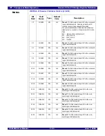
Each of the six on-chip PLLs generates a 250 MHz clock. The output of any of these PLL clocks divided
by four (i.e., a 62.5 MHz clock) may be output on GPIO alternate function pins. In addition, the 2.5 GHz
recovered SerDes receive clock from any of the 24 lanes divided by 40 (i.e., 62.5 MHz) may be selected.
SerDes Test Clock 0 (TSTCLK0) is an alternate function of GPIO[6]. The clock output on this alternate
function is selected by the Test Clock 0 Select (TSTCLK0SEL) field in the SWCTL register. SerDes Test
Clock 1 (TSTCLK1) is an alternate function of GPIO[7]. The clock output on this alternate function is
selected by the Test Clock 1 Select (TSTCLK1SEL) field in the SWCTL register.
Содержание 89HPES12N3
Страница 10: ...IDT Table of Contents PES12N3 User Manual iv June 7 2006 Notes...
Страница 14: ...IDT List of Figures PES12N3 User Manual viii June 7 2006 Notes...
Страница 36: ...IDT Clocking Reset and Initialization Reset PES12N3 User Manual 2 8 June 7 2006 Notes...
Страница 40: ...IDT Link Operation Slot Power Limit Support PES12N3 User Manual 3 4 June 7 2006 Notes...
Страница 50: ...IDT Switch Operation Switch Core Errors PES12N3 User Manual 4 10 June 7 2006 Notes...
Страница 54: ...IDT Power Management Active State Power Management PES12N3 User Manual 5 4 June 7 2006 Notes...
Страница 62: ...IDT Hot Plug and Hot Swap Hot Swap PES12N3 User Manual 6 8 June 7 2006 Notes...
Страница 78: ...IDT SMBus Interfaces Slave SMBus Interface PES12N3 User Manual 7 16 June 7 2006 Notes...
Страница 142: ...IDT Transparent Mode Operation Generic PCI to PCI Bridge Register Definition PES12N3 User Manual 9 62 June 7 2006 Notes...
Страница 148: ...IDT Test and Debug SerDes Test Clock PES12N3 User Manual 10 6 June 7 2006...
Страница 158: ...IDT JTAG Boundary Scan Usage Considerations PES12N3 User Manual 11 10 June 7 2006 Notes...


