P.6.3.1
Priority Encoder and Decoder: Circuit Description
The priority encode circuit uses an eight-to-three line Priority
Encoder (U44), a three-to-eight line decoder (U42), and three
inverters (U43).
The encoder U44 is enabled at all times, and the decoder U42
is configured so that a single logic input at pin 4 enables or
disables the decoder.
P.6.3.1.1
Encoder
For each encoder input (D2 through D7), there is a correspond-
ing binary “code” on the three output lines (A0 through A2). If
more than one input is active (logic LOW), the highest priority
input will determine the output “code.” When a higher priority
input occurs, the output lines will immediately change to the
new binary code required by the new input. The encoder,
therefore, selects the highest priority input and provides its
binary code on the three output lines.
P.6.3.1.2
Inverters
The encoder output signals are inverted by U43-8/10/12, then
go to the decoder “select” inputs (A, B, and C).
P.6.3.1.3
Decoder
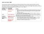
When U42 is enabled at pin 4, it will convert the encoded 3-bit
logic signal at the A, B, and C inputs back to a logic LOW signal
on one output. If more than one command occurs at the same
time, only the highest priority command will appear at the
decoder output. If NO commands are active, all decoder outputs
will be HIGH.
P.6.3.1.4
Inhibit Decode One-shot (U56B)
Decoder operation is inhibited by U56-5 for approximately .25
seconds after any OFF command is given. This prevents any
new command from operating, and prevents rapid ON/OFF
cycling of the transmitter PA Power Supply.
When an “OFF” command is latched by U40, the “OFF” output
at U40-2 goes HIGH. The “OFF” signal is buffered by U39-3
and fed to one-shot timer U56-10. The positive-going transition
triggers output U56-5 HIGH and inhibits the decoder for .25
seconds.
The Q output remains high during the one-shot’s time-out (.25
seconds), unless a supply fault clears the one shot. The time-out
(pulse width) is determined by resistor R62 and capacitor C82
at U56-7. If a Supply Fault logic signal is generated during this
time, U56-11 goes LOW and immediately clears the one-shot,
causing the Q output to go LOW again.
P.6.3.1.5
Decoder U42 Outputs
Only one decoder output can be active at a time, at the Y2
through Y7 outputs of U42. When any command is present that
output is logic LOW. If no command is present, all six outputs
will be HIGH. Because commands are only pulses (except for
“Raise” and “Lower” commands), all outputs will be HIGH
most of the time.
The OFF, HIGH, MED, and LOW outputs from the decoder go
directly to 4-input OR gate U57-8 and then to the “Power Level
Change” circuit which generates a delayed pulse to “strobe” the
Power Level Data latches on the Analog Input Board.
P.6.3.1.6
Inverters (U41-2/4/6/8/10/12)
All six Decoder outputs are inverted by the six sections of Hex
Inverter U41. When a command is present the inverter output is
logic HIGH. The inverter outputs for “Raise” and “Lower” com-
mands are not latched, and go to Up/Down Counter input gates.
“Raise” and “Lower” commands are active as long as the RAISE
or LOWER button is held, a remote command input is present, or
when the VSWR Induced Lower command is present.
Inverter outputs for Power Level commands OFF, LOW, ME-
DIUM, or HIGH go to Power Level Latch U40. The “Off”
command also goes Q5-13.
P.6.4
“Power Level Change” Pulse
Each time a new Power Level Command is decoded, a delayed
“Power Level Change” logic LOW pulse is generated by this
circuit. This pulse clocks the Power Level Latch (U40) so that
the new power level is stored, and is one of several signals that
strobe the latches on the Analog Input Board to store the new
BCD power output data.
Whenever a new power level is decoded by U42, a 20 millisec-
ond delay timer starts (R44/C77/U55-4B) and at the end of that
time-out, a 10 millisecond Power Level Change pulse (Logic
LOW) is generated at the output of U57 which latches the
command in U40. Transistor circuit Q5-14 starts a new Power
Level Change pulse immediately if an OFF command is gener-
ated while the LOW, MEDIUM or HIGH command is still
present at the input (this turns the transmitter off if a Type 1
Fault occurs during turn-on).
P.6.4.1
Inhibit
A “Supply Fault-L” output from the regulator fault summary
circuit inhibits U57-6 and prevents a “Power Level Change”
pulse.
P.6.4.2
Data Strobe
The Power Level Change pulse is “OR’ed” with other logic
signals in U13-8 (shown on sheet 3 of the schematic) to form
the Data Strobe pulse. This pulse clocks the digital power level
data latches on the Analog Input Board.
P.6.5
Power Level Latch (U40)
The OFF, LOW, MEDIUM, and HIGH commands are short
pulses. The power level latch U40 stores the power mode
information, that is, it “remembers” the last command. The latch
supply voltage is the +5B memory backup supply. This ensures
that the current “Power Level” information is still available to
restore transmitter operation after a power failure.
P.6.5.1
Power Level Latch “Clear”
The power level latch is CLEARED only if the backup supply
voltage decreases to near the level where latch operation be-
comes unreliable and integrity of stored information would be
compromised. The latch “CLEAR” input is a “RESET-L” signal
from the +5B Reset circuit (U37).
P.6.6
Latched “Off” Command
When an “OFF” command is stored, a logic HIGH output
appears at U40-2. This output is buffered by U39-3 and goes to:
DX-25U
P-8
888-2297-002
Rev. S: 05-02-97
WARNING: Disconnect primary power prior to servicing.
Содержание DX 25U
Страница 2: ......
Страница 10: ......
Страница 28: ......
Страница 32: ......
Страница 46: ......
Страница 58: ......
Страница 82: ......
Страница 150: ......
Страница 158: ......
Страница 166: ......
Страница 174: ......
Страница 176: ......
Страница 196: ......
Страница 206: ......
Страница 212: ......
Страница 218: ......
Страница 270: ......


