UPPER LEVEL ASSEMBLY: Theory of Operation
Revision D
APEX Telemetry Transmitter
6-9
401566-166
The VCO section generates a frequency based on the tuning voltage from
the loop filter. A form of Colpitts oscillator is used, with the oscillator
output frequency being controlled by the varactor diode CR1 (for -001/
002/003 and CR9 for -004) capacitance value. The capacitance of CR1
(CR9) is combined with the capacitance from C26, C30, C31 and the
capacitance from Q3 to form an equivalent capacitance in parallel with
inductor L5 (for -001/002/003 and L23 for -004) that creates a resonant
circuit. This resonant circuit frequency is amplified by transistor Q3,
then split by resistors R37, R52, and R53. One signal is input to the
frequency doubler stage and the other to the FIN port (pin 10) of PLL U2.
Capacitors C30 and C31 are also used for AC feedback and as a phase
shifting network that creates the necessary 180 degree phase shift from
the emitter of Q3 (pin 2) to the base of Q3 (pin 1) that sustains
oscillation. Capacitors C37 and C38 and inductor L12 (for -001/002/003
and L24 for -004) impedance match the output impedance of Q3 to the
input impedance of the R37/R52/R53 circuit (50
Ω
) for maximum power
transfer.
Frequency Doubler
The frequency doubler section doubles the frequency of its input (i.e., the
output signal from the VCO). Transistor amplifier Q4 operates
nonlinearly to increase the level of the VCO harmonics generated in the
amplifier. The amplifier output is tuned to the second harmonic of the
VCO using C32, C33, C39, and L10 as a tuned tank circuit.
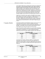
Input to the frequency doubling amplifier is a low-pass filter consisting of
C35, C36, C43, L11, and L14. The corner frequency of this low-pass filter
is presented in the table below. It is used to isolate the frequency
modulator section and the output amplifier section from the VCO section.
The output of the frequency doubling amplifier is a high-pass filter
formed from C20, C27, C28, L7, and L8. The corner of this filter is
presented in the table below. This filter isolates the frequency modulator
section from the VCO section and attenuates the VCO signal input to the
modulator.
Frequency Doubler
Assembly
Low Pass Frequency
–001
120 MHz
–002
160 MHz
–003
120 MHz
–004
300 MHz
Frequency Doubler
Assembly
High Pass Frequency
–001
150 MHz
–002
175 MHz
–003
150 MHz
–004
350 MHz
Содержание Marquette 418793-001
Страница 1: ...APEX Telemetry Transmitter Service Manual 401566 166 Revision D ...
Страница 8: ...CONTENTS vi APEX Telemetry Transmitter Revision D 401566 166 ...
Страница 100: ...TRANSMITTER PCB Schematic Diagram PN SD801278 001A 7 30 APEX Telemetry Transmitter Revision D 401566 166 Sheet 7 of 13 ...
Страница 101: ...TRANSMITTER PCB Schematic Diagram PN SD801278 001A Revision D APEX Telemetry Transmitter 7 31 401566 166 Sheet 8 of 13 ...
Страница 102: ...TRANSMITTER PCB Schematic Diagram PN SD801278 001A 7 32 APEX Telemetry Transmitter Revision D 401566 166 Sheet 9 of 13 ...
Страница 103: ...TRANSMITTER PCB Schematic Diagram PN SD801278 001A Revision D APEX Telemetry Transmitter 7 33 401566 166 Sheet 10 of 13 ...
Страница 104: ...TRANSMITTER PCB Schematic Diagram PN SD801278 001A 7 34 APEX Telemetry Transmitter Revision D 401566 166 Sheet 11 of 13 ...
Страница 105: ...TRANSMITTER PCB Schematic Diagram PN SD801278 001A Revision D APEX Telemetry Transmitter 7 35 401566 166 Sheet 12 of 13 ...
Страница 106: ...TRANSMITTER PCB Schematic Diagram PN SD801278 001A 7 36 APEX Telemetry Transmitter Revision D 401566 166 Sheet 13 of 13 ...
Страница 122: ...OXIMETER ASSEMBLY Parts Location Diagram 421191 001A 8 14 APEX Telemetry Transmitter Revision D 401566 166 Sheet 2 of 3 ...
Страница 123: ...OXIMETER ASSEMBLY Parts Location Diagram 421191 001A Revision D APEX Telemetry Transmitter 8 15 401566 166 Sheet 3 of 3 ...


