76 PPC11A 6U VME Single Board Computer
Publication No. PPC11A-HRM/1
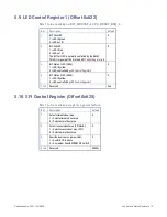
5.11
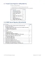
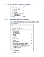
PCIe SATA SPI Control Register (Offset 0x626)
Bits
Description
Default
7
PCIe SATA SPI programming enable:
1 = Programming enabled
0 = Programming disabled
0
6
PCIe SATA SPI hold:
1 = Hold
0 = Do not hold
1
5
PCIe SATA SPI write protection status:
1 = Write protection is active
0 = Write protection is not active
1
4 to 0
Reserved
00000
b
5.12
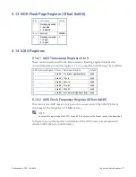
BIT Control/Status Register (Offset 0x629)
Apart from bits 7 and 1, this register has no effect within the FPGA; it is provided
solely for BIT software to store its context. Bits 6 to 2 and 0 are sticky unless the reset
cause is a power failure.
Bits
Description
Default
7
BIT_HRESET
a
request:
1 = Board reset requested
0 = No board reset requested
This bit clears itself after the reset occurs
0
6 & 5
BIT Run Status:
00
b
= BIT not previously run
01
b
= Fast BIT performed
10
b
= Full BIT performed
11
b
= Fast Start performed
00
b
4
BIT Pass/Fail:
1 = BIT failed
0 = BIT passed
1
3
Fast BIT:
1 = Fast BIT enabled
0 = Fast BIT disabled
0
2
Fast Start:
1 = Fast Start enabled
0 = Fast Start disabled
0
1
Controls whether BIT_HRESET request also causes SYSRESET:
1 = BIT_HRESET request also causes a SYSRESET output
0 = BIT_HRESET request does not cause a SYSRESET output (default)
This is independent of whether the PPC11A is System Controller.
By itself, this bit does not generate a reset of any kind
(BIT_HRESET has that function)
0
0
BIT run:
1 = BIT has been run
0 = BIT has not been run
0
a.
The name “_HRESET” is retained from the common Haswell register set, although in fact this generates a
PORESET in Freescale terminology.
Содержание PPC11A
Страница 1: ...Hardware Reference Manual PPC11A 6U VME Single Board Computer Edition 1 Publication No PPC11A HRM 1 ...
Страница 27: ...Publication No PPC11A HRM 1 Functional Description 27 Figure 4 2 Block Diagram T2081 ...
Страница 113: ...Publication No PPC11A HRM 1 Connectors 113 Figure 6 2 Rear Connector Position ...


