background image

28 PPC11A 6U VME Single Board Computer 


Publication No. PPC11A-HRM/1 

Figure 4-3 Block Diagram (T1042) 

  NOTES 

1.


Due to the increasingly short lifetimes of system components, the I/O devices used on the PPC11A are 

not guaranteed to remain fixed in the future. 

2.


Hardware should be accessed only through mechanisms provided by the Operating System’s Board 

Support Package, and not directly by application software. 

3.


If a standard operating system is not being used, then it is recommended that applications are written 

in such a way as to minimize direct access to hardware resources, bearing in mind that changes may 

be necessary to support future iterations of the hardware. 

4.


Abaco-supported Operating Systems guarantee compatibility at the application level through 

hardware independent mechanisms. 

Содержание PPC11A

Страница 1: ...Hardware Reference Manual PPC11A 6U VME Single Board Computer Edition 1 Publication No PPC11A HRM 1 ...

Страница 2: ...oved Producer Compliance Scheme PCS and subject to suitable contractual arrangements being in place will ensure WEEE is processed in accordance with the requirements of Directive 2012 19 EU of the European Parliament of 4 July 2012 on Waste Electrical and Electronic Equipment Abaco Systems Limited will evaluate requests to take back products purchased by our customers before August 13 2005 on a ca...

Страница 3: ...e the latest version Further Information Abaco Website You can find information on Abaco products on the following website LINK https www abaco com Abaco Documents You may register for access to manuals via the website whose link is given above LINKS PMC XMC Installation Application Note publication number HN4 5 16 P0P2X605 Product Manual publication number P0P2X605 HRM I O Modules Hardware Refere...

Страница 4: ...t of the specifications and data sheets that provide any additional information required follows Specifications IEEE 1101 1 1998 IEEE Standard for Mechanical Core Specifications for Microcomputers IEEE 1101 2 1992 Conduction cooled VME mechanics IEEE 1101 10 1996 Additional Mechanical Specifications ANSI VITA 20 2001 Conduction Cooled PMC ANSI VITA 32 2003 Processor PMC ANSI VITA 39 2003 PCI X for...

Страница 5: ... build levels 1 and 2 and at least 600 lfm for build level 3 If a conduction cooled level 4 or 5 PPC11A is operating on an extender card it requires air flow of at least 300 lfm across it Handling CAUTION Only handle the PPC11A by the edges or front panel ESD Label Present on Board Packaging Heatsink CAUTIONS Do not remove the heatsink There are no user alterable components underneath the heatsink...

Страница 6: ...5 Mezzanine Installation 22 3 Installation and Power Up Reset 24 3 1 Power Supply Requirements 24 3 2 Board Installation Notes 24 3 3 Connecting to PPC11A 25 3 3 1 Rear Transition Module 25 3 4 Reset and Power up Sequence 25 4 Functional Description 26 4 1 Introduction 26 4 2 Features 29 4 3 Integrated Host Processor 30 4 3 1 Processor Features 30 4 3 2 PowerPC Processing Cores 30 4 3 3 Trust Arch...

Страница 7: ... 16 MIL STD 1553 46 4 17 Graphics 47 4 17 1 VGA 47 4 17 2 DVI 47 4 18 Mezzanines 48 4 18 1 PMC XMC Sites 48 4 18 2 PMCs 48 4 18 3 XMCs 49 4 18 4 I O Routing 49 4 18 5 PMC XMC Site 1 Configuration 49 4 18 6 PMC XMC Site 2 Configuration 51 4 19 PCIe Infrastructure 52 4 19 1 Processor 52 4 19 2 PCIe Switches 53 4 20 I2 C Buses 55 4 20 1 Main Bus 55 4 20 2 Sensor and Backplane Buses 56 4 20 3 I2 C Bus...

Страница 8: ... Offset 0x64E 77 5 14 3 AXIS Clock Control Register Offset 0x64F 78 5 15 Timer Registers 78 5 15 1 Timer 0 Control Status Register 1 Offset 0x650 Timer 1 Control Status Register 1 Offset 0x658 Timer 2 Control Status Register 1 Offset 0x660 and Timer 3 Control Status Register 1 Offset 0x668 78 5 15 2 Timer 0 Control Status Register 2 Offset 0x651 Timer 1 Control Status Register 2 Offset 0x659 Timer...

Страница 9: ...ister Offset 0x692 87 5 18 12 GPIO 23 16 Test Mode Register Offset 0x693 87 5 19 GPIO Availability Debug Register Offset 0x694 87 5 20 Availability Registers 88 5 20 1 Ethernet Availability Register Offset 0x6A0 88 5 20 2 COM Port Availability Register Offset 0x6A1 88 5 20 3 COM Port 4 Wire Configuration Register Offset 0x6A2 89 5 20 4 COM Port Modem Configuration Register Offset 0x6A3 89 5 20 5 S...

Страница 10: ...figuration Unlock Password Register Offset 0x6EC 106 5 45 Control Register Offset 0x6ED 106 5 46 Scratch Pad Register 2 Offset 0x6EE 106 5 47 LED Control Register 2 Offset 0x6EF 106 5 48 Flash Password Registers Offsets 0x6F0 to 0x6F7 107 5 49 EEPROM DIP Switch 2 Configuration Register 1 Offset 0x6FA 107 5 50 EEPROM DIP Switch 2 Configuration Register 2 Offset 0x6FB 107 5 51 Watchdog Registers 107...

Страница 11: ...tion 127 A 2 Electrical Specification 128 A 3 Reliability MTBF 129 A 4 Mechanical Specification 129 A 5 Product Codes 130 A 6 Software Support 131 A 6 1 Boot Firmware 131 A 6 2 Built In Test 131 A 6 3 Background Condition Screening 132 A 7 I O Modules 132 A 8 Test Access Card 132 A 9 Development Systems 132 B Statement of Volatility 133 B 1 Volatile Memory 133 B 2 Non Volatile Memory 133 C PPCx Co...

Страница 12: ...C11A HRM 1 C PPCx Compatibility continued C 4 PPC10A 148 C 4 1 P0 Connector 148 C 4 1 P0 Connector Alternative 149 C 4 2 P1 Connector 150 C 4 3 P2 Connector 151 C 4 1 P2 Connector Alternative 1 152 C 4 1 P2 Connector Alternative 2 153 Glossary 154 Index 155 ...

Страница 13: ...gnal Routing 42 Table 4 12 COM5 Signal Routing 43 Table 4 13 COM6 Signal Routing 43 Table 4 14 USB0 USB1 Signal Routing 43 Table 4 15 SATA Signal Routing 44 Table 4 16 GPIO Line Routing 45 Table 4 17 MIL STD 1553 Routing 46 Table 4 18 VGA Routing 47 Table 4 19 DVI Routing 47 Table 4 20 PMC XMC Site 1 Signal Availability 50 Table 4 21 PMC Site 2 1 46 Signal Availability 51 Table 4 22 PMC Site 2 47 ...

Страница 14: ...23 Pin Assignments 120 Table 6 9 J14 Pin Assignments 121 Table 6 10 J24 Pin Assignments 121 Table 6 11 PMC Signal Descriptions 122 Table 6 12 J15 J25 Pin Assignments 123 Table 6 13 J16 Pin Assignments 124 Table 6 14 XMC Signal Descriptions 125 Table A 1 Technical Data 127 Table A 2 Voltage Supply Requirements 128 Table A 3 Current Consumption 128 Table A 4 Reliability MTBF 129 Table A 5 Mechanical...

Страница 15: ...am T2081 27 Figure 4 3 Block Diagram T1042 28 Figure 4 4 Ethernet PHY Block Diagram 40 Figure 4 5 RS422 485 Signal Definition 41 Figure 4 6 I2 C Main Bus Structure 55 Figure 4 7 I2 C Sensor Backplane Bus Structure 56 Figure 4 8 I2 C Bus 3 Structure 57 Figure 4 9 JTAG Chains 65 Figure 4 10 LED Positions 66 Figure 4 11 Conduction cooled Front Panel 68 Figure 4 12 0 8 Air cooled Front Panel 69 Figure...

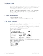
Страница 16: ...SLA 001 01 1 2 Identifying Your Board The PPC11A is identified by labels at strategic positions These can be cross checked against the Advice Note provided with your delivery Identification labels like the example shown in Figure 1 1 attached to the shipping box and the antistatic bag give identical information product code product description equipment number and board revision Figure 1 1 Product...

Страница 17: ...s 4 and 5 there is also a label like the example shown in Figure 1 3 attached to the front of the heatsink Figure 1 3 Product Label Conduction cooled Product See the Product Codes section in Appendix A for more details on the product code PPC11A xxxxxxxx PPC11A CAGE CODE K7034 MADE IN UK 48C111B4 ...

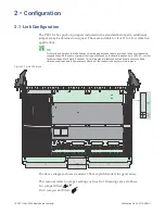
Страница 18: ...n the pin posts and then cover these wire wrapped links with the same conformal coating as that used on the board usually Acrylic 1B73AP contact Technical Support for details if needed This will provide a reliable connection under heavy shock and vibration conditions and further prevent oxidation of the connection due to moisture ingress Figure 2 1 Link Positions The above diagram shows standard 2...

Страница 19: ...sections allowing for three different boot images to be loaded into the Flash There is also an Abaco programmed Recovery boot image which is stored in a separate SPI Flash These links are used to select which image is used at boot time Table 2 1 P15 Pins 1 to 4 Jumper Functions Pins 1 and 2 Pins 3 and 4 Active Boot Image Out Out Main In Out Alternate Out In Recovery In In Reserved In normal operat...

Страница 20: ...wing a reset or a power cycle to be altered See the Flash Sector Protection section for more details Not fitting a jumper on this link prevents software from altering any previously configured sector protection Table 2 3 P15 Pins 7 and 8 Jumper Function Setting Meaning Out Persistent sector protection cannot be altered In Persistent sector protection can be altered NOTE When selected using EEPROM ...

Страница 21: ...d 16 Jumper Functions Setting Meaning Out PMC site 2 VIO signaling voltage is 3 3V In PMC site 2 VIO signaling voltage is 5V These links should only be fitted when a PMC that uses 5V signaling is installed and should be left not fitted otherwise 2 3 6 Reserved Links P17 and P18 These are reserved for use by Abaco only Do not fit jumpers on these links 2 4 Software Board Configuration The PPC11A co...

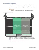
Страница 22: ...or the fitting of two single width PMCs XMCs or one double width PMC XMC CAUTION Ensure that the PMC1 and PMC2 5V VIO configurations are set according to the requirements of the corresponding PMC s Damage to the PMC s may otherwise result Figure 2 2 PMC XMC Site Locations A PMC XMC supplied by Abaco is delivered with a kit of parts for mounting it A PMC XMC ordered with a PPC11A can be supplied fi...

Страница 23: ... Where a PMC XMC is not pre installed prove operation of the PPC11A before installing the PMC XMC NOTE The power dissipation of any XMC fitted should be considered An XMC with high power dissipation could cause the temperature of the PPC11A to rise beyond an acceptable limit The magnitude of the effect of the XMC largely depends on the XMC thermal solution and needs to be considered on a case by c...

Страница 24: ...1 The VME specification allows for a variety of different backplane pinouts depending on the I O configuration selected Ensure that the PPC11A pinout matches that of the backplane slot before insertion 2 Air cooled versions of the PPC11A have injector ejector handles to ensure that the backplane connectors mate properly with the backplane The captive screws at the top and bottom of the front panel...

Страница 25: ...to provide two 9 way D type connectors for COM1 COM2 A null modem 9 way D type cable for connecting COM1 to a control terminal or PC running terminal emulation software For the Ethernet ports a CAT5 or better straight through patch cable for 10 100 1000BASE T The I O Modules manual contains more details on fitting the RTM Similar antistatic and safety precautions apply when handling and or install...

Страница 26: ...Gigabit Ethernet channels serial COMs USB2 0 and Serial ATA interfaces A VME64 interface is available to the backplane The processor is connected to PCI devices and mezzanine sites using PCIe through a non blocking switch architecture Two 64 bit PMC sites are provided each supporting PCI X operation at up to 133 MHz allowing for off the shelf or custom PMCs to be fitted to add further functionalit...

Страница 27: ...Publication No PPC11A HRM 1 Functional Description 27 Figure 4 2 Block Diagram T2081 ...

Страница 28: ... mechanisms provided by the Operating System s Board Support Package and not directly by application software 3 If a standard operating system is not being used then it is recommended that applications are written in such a way as to minimize direct access to hardware resources bearing in mind that changes may be necessary to support future iterations of the hardware 4 Abaco supported Operating Sy...

Страница 29: ...terface has a 64 bit PCI PCI X interface and can operate at up to 133 MHz Each XMC interface has a x4 Gen2 PCIe link PCIe interconnect with non blocking switch architecture VME64x interface to VME P1 P2 Two 10 100 1000BASE T Ethernet ports plus two optional 10 100 1000BASE T Ethernet ports Up to six serial COM ports Up to two USB 2 0 ports Up to two SATA ports Up to two dual redundant MIL STD 1553...

Страница 30: ...ng Point Unit MMU with embedded Hypervisor privilege level Table 4 2 Processor Frequencies Processor Type Core Frequency Platform Frequency Memory Bus Frequency T1042 1 4 GHz 600 MHz 800 MHz T2081 1 8 GHz 600 MHz 800 MHz Depending on the application it is possible for software to dynamically configure processors to run at lower clock frequencies to minimize power 4 3 3 Trust Architecture The T2081...

Страница 31: ... frequency and numerous configuration options of the processor Normally the RCW is loaded from Abaco configured settings within the FPGA and no user interaction is required If more sophisticated configuration is required it is possible to load the data structure from an I2C EEPROM instead by setting the relevant software configuration option in the I2C EEPROM DIP Switch CAUTION Do not change the s...

Страница 32: ...local bus are made available shared between the devices as defined in the table below The minimum possible window size is 32 KB Table 4 3 Local Bus Chip Select Targets Chip Select Target Device Width Required Window Size CS0 Top half NOR Flash Boot area 2x8MB Bottom half RCW in FPGA 16 bit 32 MB CS1 NOR Flash 16 bit 256 MB CS2 NVRAM 8 bit 512 KB CS3 FPGA registers 8 bit 4 KB CS4 FPGA UART BMM 8 bi...

Страница 33: ...trols the frequency of the RAM interface Table 4 2 shows the possible configurations 4 4 2 Serial Presence Detect The PPC11A implements a mechanism like the JEDEC DDR3 SPD to indicate the RAM layout and timing information to the system The SPD uses a virtual I2C ROM that is embedded within the FPGA 4 5 NOR Flash The PPC11A provides 512 MB of Flash memory connected to the processor using the Local ...

Страница 34: ...tion to ensure the integrity of code data contained in the Flash array Protection is defined on a per sector basis where a sector is 128 KB in size Locked sectors cannot be erased or programmed they may only be read No write protection of Flash is provided by hardware Software must be used to configure the Flash devices to protect against corruption of Flash data The following types of protection ...

Страница 35: ...ice is an SLC mode type which is MLC technology operating to give similar endurance and retention as pure SLC operation Alternative devices sizes and Flash technologies are available LINK For more details on the SSD see http www siliconmotion com The SSD may be write protected using an output from the EEPROM DIP Switch 1 Register 0 Software is also able to trigger a fast erase of the device using ...

Страница 36: ... controller 4 9 1 VMEbus Compliance Table 4 6 VMEbus Compliance Component Description Master A16 A24 A32 and A64 D08 EO D16 and D32 Single Cycle Transaction SCT D08 EO D16 and D32 Read Modify Write Transaction RMW D16 and D32 Block Transaction BLT D64 Multiple Block Transaction MBLT Slave A16 A24 A32 and A64 D08 EO D16 and D32 Single Cycle Transaction SCT D08 EO D16 and D32 Block Transaction BLT D...

Страница 37: ... A24 or A16 space An offset may be applied to translate the VMEbus address to a different address on the local bus allowing any VMEbus address to access any on board address The start address and size of window are programmable VMEbus slave accesses to the PPC11A may be coupled write posted or pre fetched block read Coupled slave transfers can only proceed once the slave posted write FIFO is empty...

Страница 38: ... ID and then raises an interrupt on the PCI bus No further VMEbus interrupts are handled on that level until the processor reads the status ID and re arms the interrupt handler The Universe II can be programmed to generate any level of VMEbus interrupt It can raise an interrupt on the PCI bus when the VMEbus interrupt has been acknowledged Seven software interrupts in the Universe II allow an inte...

Страница 39: ...tiator requests a coupled cycle to the VMEbus while the posted write FIFO still contains data The PCI initiator requests a posted write cycle when the posted write FIFO can accept no more entries The Universe II does not support the VMEbus RETRY signal 4 10 I O The PPC11A has the following I O connectivity Ethernet Serial Ports USB Serial ATA General Purpose I O MIL STD 1553 VGA and DVI graphics D...

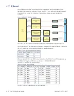
Страница 40: ...ithin Frame Manager 2 as shown below Table 4 7 Processor Network Interface Mapping Processor Module Ethernet Port PHY Address FM2_dTSEC3 ETH0 1 FM2_dTSEC4 ETH1 3 Ethernet ports ETH0 and ETH1 are provided on the VME P2 and P0 connectors as 10 100BASE T option PPC11A xxxxx2xx or 10 100 1000BASE T option PPC11A xxxxx1xx as follows Table 4 8 ETH0 ETH1 Pin Mapping 10 100 Signal 1000BASE T Signal P2 Pin...

Страница 41: ...co and may be displayed by software LEDs on the rear of the board show the status of each Ethernet interface 4 12 Serial Communication Ports The PPC11A provides up to six external serial ports 4 12 1 COM1 and COM2 The processor s DUART interface provides two debug ports with RTS CTS hardware flow control The signals for these ports are connected to ISL41334 serial transceivers capable of generatin...

Страница 42: ...ad UART connected to the processor via a PCIe Switch These ports are capable of operation in RS232 422 485 in both synchronous and asynchronous modes providing support for SDLC and HDLC protocols The serial ports are driven by ISL41334 bus transceivers and can be configured by software to operate in RS232 RS422 or RS485 modes In RS485 mode the serial controller can automatically disable the transm...

Страница 43: ... COM6_TXD_A D11 COM6_RTS COM6_TXD_B COM6_TXD_B D12 COM6_RXD COM6_RXD_A COM6_RXD_A D23 COM6_CTS COM6_RXD_B COM6_RXD_B D24 4 12 3 Host to BMM Serial Port The FPGA contains an IP core for a 16550 compatible UART which may be used by software running on the host processor to communicate with the BMM if required 4 13 USB The processor provides two USB2 0 ports to the P2 connector Power for these ports ...

Страница 44: ...al P0 Pin SATA_TX0P A9 SATA_TX1P B9 SATA_TX0N A11 SATA_TX1N B11 SATA_RX0P D9 SATA_RX1P E9 SATA_RX0N D11 SATA_RX1N E11 LEDs on the rear of the board show activity on the corresponding SATA channel 4 15 GPIO The PPC11A supports up to 19 GPIO lines each with interrupt generation capabilities They are all 3 3 V single ended signals with 5 V tolerance Up to 19 lines are controlled by the FPGA and can b...

Страница 45: ...C14 7 P2 A8 P2 C15 P2 C15 P2 C15 8 P2 A9 P2 C16 P2 C16 9 P2 A10 P2 C17 P2 C17 10 P2 A11 P2 C18 P2 C18 11 P2 A12 P2 C19 P2 C19 12 P2 A13 P2 C20 P2 C20 13 P2 A14 P2 C21 P2 C21 14 P2 A15 P2 C22 P2 C22 15 P2 A16 P2 C23 P2 C23 16 P2 A17 P2 C24 P2 C24 17 P2 A18 P2 C25 P2 C25 18 P2 A19 P2 C26 P2 C26 Depending on the setting of EEPROM DIP Switch 1 Register 1 GPIO 7 4 can be configured to have alternate fu...

Страница 46: ...ng to the P2 connector Table 4 17 MIL STD 1553 Routing MIL STD 1553 Signal Pin MIL STD 1553 Signal Pin CH0_1553_IDCSAP A1 CH1_1553_IDCSAP A28 CH0_1553_ITCSAP A2 CH1_1553_ITCSAP A29 CH0_1553_ISGNDA A3 CH1_1553_ISGNDA A30 CH0_1553_ITCSAN A4 CH1_1553_ITCSAN A31 CH0_1553_IDCSAN A5 CH1_1553_IDCSAN A32 CH0_1553_EXT_TRIG A6 CH1_1553_EXT_TRIG A14 CH0_1553_RT_BOOT A7 CH1_1553_RT_BOOT A13 CH0_1553_IDCSBP A8...

Страница 47: ... section for more details The following table shows the VGA routing to the P2 connector Table 4 18 VGA Routing Signal Pin VGA_RED A30 VGA_GREEN A31 VGA_BLUE A32 VGA_HSYNC A28 VGA_VSYNC C7 4 17 2 DVI DVI output is available with options PPC11A xxxx2xxx PPC11A xxxx4xxx PPC11A xxxx5xxx and PPC11A xxxx7xxx see the Product Codes section for more details The following table shows the DVI routing to the ...

Страница 48: ...ericom PI7C9X130 PCI Express to PCI Bridge which provides clocks and arbitration for the bus The speed of the bus is based on the capability of the PMC and is determined by the bridge during reset The current operating frequency of each bus may be ascertained by reading registers within the appropriate bridge The PMC_PRESENT signal from each site is used to hold the respective PCIe to PCI bridge i...

Страница 49: ...The I O from PMC connector J14 pins is tracked as 50Ω single ended signals matched in length in groups of eight signals 1 8 9 16 etc but not as differential pairs such that it may support differential signaling for Ethernet etc but not cause cross talk problems with cards that use single ended I O The I O from XMC connector J16 columns A B D and E is tracked as 100Ω differential pairs A01 and B01 ...

Страница 50: ...11 E6 P14_IO_43 C15 P16_IO_F12 A5 P16_IO_D11 E15 P16_IO_B17 A18 P14_IO_12 D6 P14_IO_44 B15 P16_IO_F13 D6 P16_IO_A05 B12 P16_IO_D17 D18 P14_IO_13 C6 P14_IO_45 A15 P16_IO_C14 C6 P16_IO_B05 A12 P16_IO_E17 C18 P14_IO_14 B6 P14_IO_46 E16 P16_IO_C15 A6 P16_IO_D05 D12 P16_IO_A19 C19 P14_IO_15 A6 P14_IO_47 D16 P16_IO_F14 B6 P16_IO_E05 C12 P16_IO_B19 B19 P14_IO_16 E7 P14_IO_48 C16 P16_IO_F15 E7 P16_IO_A07 ...

Страница 51: ...24_IO_56 D9 P24_IO_2 Z1 P24_IO_25 D17 P24_IO_48 A10 P24_IO_57 E11 P24_IO_3 D2 P24_IO_26 Z17 P24_IO_49 B9 P24_IO_58 D11 P24_IO_4 D3 P24_IO_27 D18 P24_IO_50 A9 P24_IO_59 C10 P24_IO_5 Z3 P24_IO_28 D19 P24_IO_51 B11 P24_IO_60 N A P24_IO_6 D4 P24_IO_29 Z19 P24_IO_52 A11 P24_IO_61 C11 P24_IO_7 D5 P24_IO_30 D20 P24_IO_53 N A P24_IO_62 C9 P24_IO_8 Z5 P24_IO_31 D21 P24_IO_54 N A P24_IO_63 E10 P24_IO_9 D6 P...

Страница 52: ... Per direction PCIe x8 2 5 Gbps 2000 Per direction PCIe Bandwidths shown include 8b 10b encoding overheads PCIe is a packet based protocol but uses the same address spaces as standard PCI meaning that the software interfaces are backwards compatible PCIe to PCI Bridges are used to convert to PCI X or standard PCI where connection to these devices is required The maximum packet payload size for the...

Страница 53: ...ernet 4 Gen1 No Down 3 Not used 11 Not used 13 14 x1 Not used No Down 15 15 x1 Not used No Down The switches are connected to I2C Bus 3 to allow configuration by the processor and out of band link status monitoring Each PCIe port of the switch appears to software as a PCI to PCI bridge with its own PCI compatible configuration registers Each port is accessed on the internal virtual PCI bus using a...

Страница 54: ...ink P15 pins 9 and 10 link The switch is prevented from accessing the EEPROM when in recovery mode so that the data may be recovered if it becomes corrupted LEDs on the rear of the PPC11A show the status of the PCIe links These are driven by I2C expanders also connected to the private I2C bus Further status information number of active lanes link speed etc can be ascertained from registers within ...

Страница 55: ...agents without intervention from the processor There is an additional I2C bus from the processor that connects to the PCIe Clock Synthesizers and the central PCIe switches Where I2C addresses are quoted in the following sections the address that would be used to write to the device on the bus is an 8 bit address consisting of the 7 bit device address given plus the LSB set to 0 4 20 1 Main Bus The...

Страница 56: ...tware disable function is provided to electrically link the processor into the Sensor bus For test purposes If the BMM is not fitted If the processor negotiates ownership of the Sensor bus with the BMM NOTE This buffer should not be used when the BMM is active since the BMM is not multi master capable Both XMC sites are normally be connected to the Sensor bus Table 4 27 I2 C Sensor Bus Addresses D...

Страница 57: ...when a slave device without a reset pin is driving out data The processor provides a software mechanism to recover from this state so no hardware recovery mechanism is provided The processor and PCIe switches apply a reset pattern to the appropriate I2C buses before configuring from their EEPROMs 4 20 5 Processor Config EEPROM A 32 KB 24LC256 EEPROM is attached to I2C Bus 1 This can store the RCW ...

Страница 58: ...ard function 1 Use GPIO7 as a duplicate Boot Recovery link input 4 Boot site swap 0 Boot from Main boot image in NOR Flash 1 Boot from Alternate boot image in NOR Flash 5 NVRAM write protect 0 Write enable NVRAM 1 Write protect NVRAM 2 0 0 XMC2 GA bit 2 For site 2 PMC deployments program these to 5D 101b to select 5V VIO Otherwise VIO is 3 3V VIO is always set to 3 3V for combined XMCs PMCs 1 XMC2...

Страница 59: ...r The PPC11A uses a Lattice L ASC10 power manager to sequence the power supplies in the required order for devices The power manager also monitors each rail and its voltage can be read from registers internal to the device across the I2C interface Table 4 30 Power Manager Monitor Points Monitor Point Supply Name Nominal Voltage Attenuation VMON1 T2081_CORE 0 9V to 1 05V x1 VMON2 P1V0 1 0V x1 VMON3...

Страница 60: ...0 ns and a maximum timeout period of 85 9 seconds assuming a 50 MHz bus speed Following reset the Watchdog timer is initially disabled It can be enabled by writing a 01 followed by 10 pattern to the relevant control register When enabled the counter is reloaded to the preset value and the reset and interrupt bits are cleared if the preset counter value is higher than the interrupt value Once enabl...

Страница 61: ...erfaces Serial UART interface connected to the FPGA accessed using CS2 Backplane System Management bus I2C on the P1 connector I2C Bus 2 for access to sensor devices I2C bus to XMC sites VME geographic address The BMM can reset or power off the PPC11A in response to a request from software running on the processor or via commands over the backplane System Management bus The BMM can control the sta...

Страница 62: ...by the FPGA is used to reset the processor including the cores and all other devices on the PPC11A that require resetting A hard reset is asserted when any of the following events occur Any of the power supplies fall outside specification The VME SYSRESET signal is asserted The processor HRESET_REQ output is asserted The front panel Reset switch is toggled when enabled in software The HRESET signa...

Страница 63: ...rnal Interrupt Pin Source Port 1 INTB IRQ 1 PCIe Switch Port 1 INTC IRQ 2 PCIe Switch Port 1 INTD IRQ 3 PCIe Switch Port 2 INT B IRQ 5 VME interface Port 2 INT C IRQ 6 VME interface Port 2 INT D IRQ 7 VME interface The INTA signals from the PCIe ports are routed as dedicated inputs to the Interrupt Controller and are not shared with external pins FPGA Interrupts The FPGA connects to the IRQ 0 IRQ ...

Страница 64: ...iming parameters for devices such as the SDRAM and the Local Bus 4 24 3 Serial Presence Detect The SPD data for the main memory array is held in a virtual I2C ROM that is embedded within the FPGA 4 24 4 AXIS Support AXIS Advanced Multiprocessor Integrated Software is a set of software modules that can be used to accelerate the design development testing and deployment of complex DSP and multiproce...

Страница 65: ... 9 JTAG Chains The PPC11A connects the backplane JTAG interface on the P1 connector to the JTAG interfaces of the VME Bridge and mezzanine sites The PPC11A provides a route through circuit so that the backplane chain continues to work if a mezzanine site is not populated If a mezzanine site is populated then the mezzanine must either implement JTAG or loop the chain through otherwise the other sit...

Страница 66: ...lication No PPC11A HRM 1 4 26 LEDs LEDs are mounted on the back of the PPC11A to reflect the status of the following functions Power Supplies BIT Reset status Ethernet links PCIe links SATA activity PCIe Switch status Figure 4 10 LED Positions ...

Страница 67: ...TH1 LED DS20 Green PCIE SW 1 Lane 3 good DS47 Yellow ETH1 LED DS21 Green PCIE SW 1 Lane 8 good DS48 Green Display GPIO_0 DS22 Green PCIE SW 1 Lane 10 good DS49 Tri color Reserved DS23 Green PCIE SW 1 Lane 12 good DS50 Green Power good on all rails DS25 Green PCIE SW 1 Lane 15 good DS51 Green MachX02 slave debug signals 0 to 6 on DS51 to DS57 respectively DS26 Red PCIE SW 1 fatal error DS52 Green D...

Страница 68: ... is present DS46 flashes In 100BASE T mode both DS46 and DS47 are lit When activity is present both DS46 and DS47 flash In 1000BASE T mode DS47 is lit When activity is present DS47 flashes 4 27 Conduction cooled Front Panel Build Levels 4 and 5 Figure 4 11 Conduction cooled Front Panel XMC PMC Sites There is no access to front I O from XMCs PMCs in a conduction cooled environment NOTE If you are f...

Страница 69: ... the PPC11A then Abaco will fit a blanking plate at the site for EMC protection If you are fitting a third party mezzanine it must comply with appropriate air cooled XMC PMC standards to ensure that it mates correctly with the PPC11A mechanics Mezzanines from Abaco comply with these standards If you are fitting a mezzanine yourself first remove the corresponding blanking plate at the desired site ...

Страница 70: ... 7 0 Interrupt Select R W 0x636 NOR Flash Page R W 0x67A GPIO 7 0 Interrupt Non Maskable R W 0x648 to 0x64D AXIS Timestamp 0 to AXIS Timestamp 5 RO 0x67B GPIO 7 0 Test Mode R W 0x64E AXIS Clock Frequency R 0x67C GPIO 15 8 Out R W 0x64F AXIS Clock Control R W 0x67D GPIO 15 8 In RO 0x650 Timer 0 Control Status 1 R W 0x67E GPIO 15 8 Direction R W 0x651 Timer 0 Control Status 2 R W 0x67F GPIO 15 8 Int...

Страница 71: ...figuration 0 RO 0x6A9 Display Availability RO 0x6EB EEPROM DIP Switch 1 Configuration 1 RO 0x6AA VGA Availability RO 0x6EC Configuration Unlock Password WO 0x6AB DVI HDMI Availability RO 0x6ED Control R W 0x6AC Display Port Availability RO 0x6EE Scratch Pad 2 R W 0x6AD Ancillary Audio Availability RO 0x6EF LED Control 2 R W 0x6AE Front Panel Configuration RO 0x6F0 to 0x6F7 Flash Password Byte 0 to...

Страница 72: ... All registers are configured as 8 bits wide and use the little endian numbering convention i e bit 7 is the MSB and bit 0 is the LSB NOTE To mitigate against any changes that may be required to the register set in the future register access should ideally be performed using operating system function calls rather than directly 5 1 Board ID Register Offset 0x600 The PPC11A board ID is 0x8E 5 2 Boar...

Страница 73: ... should be written to read bytes until NULL is encountered or the last byte 0x61A is reached 5 6 Reset Cause Register 1 Offset 0x61B For the non reserved bits 1 The last reset was caused by the named event 0 The last reset was not caused by the named event default Bits Reset Cause Default 7 A power failure 6 XMC1 XMC1_RESET_OUT_L 5 XMC2 XMC2_RESET_OUT_L 4 Reserved 0 3 Software BIT_HRESET is set in...

Страница 74: ...the BIT Fail LED see the LED Control Register The BMM normally controls the BIT Fail LED only set this bit if the BMM is not populated 1 Enable BIT Fail LED output from FPGA 0 Disable BIT Fail LED output from FPGA 0 6 Reserved 0 5 BMM serial port mode 1 BMM Serial port disabled 0 BMM Serial port enabled normal operation This value is driven out unaltered to the BMM_SERIAL_MODE output pin 0 4 BMM_P...

Страница 75: ...us 1 LED DS44 1 LED lit yellow 0 LED controlled by LED Control Register 2 0 4 BIT Status 2 LED DS45 1 LED lit yellow 0 LED controlled by LED Control Register 2 0 3 to 0 Reserved 0x0 5 10 SPI Control Register Offset 0x625 Bits 7 to 5 are sticky except on a power failure Bits Description Default 7 Select alternate boot area 1 Select alternate boot area 0 Select normal boot area 0 6 Select recovery b...

Страница 76: ... 1 Board reset requested 0 No board reset requested This bit clears itself after the reset occurs 0 6 5 BIT Run Status 00b BIT not previously run 01b Fast BIT performed 10b Full BIT performed 11b Fast Start performed 00b 4 BIT Pass Fail 1 BIT failed 0 BIT passed 1 3 Fast BIT 1 Fast BIT enabled 0 Fast BIT disabled 0 2 Fast Start 1 Fast Start enabled 0 Fast Start disabled 0 1 Controls whether BIT_HR...

Страница 77: ...ys be read first AXIS Timestamp Register Offset Timestamp Value Bits Default 0 0x648 7 to 0 least significant byte 0x00 1 0x649 15 to 8 0x00 2 0x64A 23 to 16 0x00 3 0x64B 31 to 24 0x00 4 0x64C 39 to 32 0x00 5 0x64D 47 to 40 most significant byte 0x00 5 14 2 AXIS Clock Frequency Register Offset 0x64E This returns the AXIS master clock period in nanoseconds When the PPC11A is clock master the freque...

Страница 78: ...set 0x650 Timer 1 Control Status Register 1 Offset 0x658 Timer 2 Control Status Register 1 Offset 0x660 and Timer 3 Control Status Register 1 Offset 0x668 Bits Description Default 7 Timer IRQ status 1 Pending 0 No interrupt N A 6 Reserved 0 5 4 Clock source select 00b Use 2 MHz FPGA clocka 01b Use 25 MHz Watchdog clock source 10b Use processor IFC bus clock 11b Reserved 00b 3 Timer Read selection ...

Страница 79: ...ption Default 7 to 5 Reserved 000b 4 Timer read latch select 1 Latch all timers on read of Timer 0 LS Byte 0 Latch individual timers on the read of individual Timer LS Byte 3 2 Reserved 00b 1 Timer One shot Enable 1 Timer will count down and stop 0 Timer will count down and reload at terminal count 0 Timer Enable 1 Timer enabled 0 Timer disabled 5 15 3 Timer 0 Interrupt Clear Register Offset 0x652...

Страница 80: ...0 Timer 0 Data Byte 1 0x65D 0x00 Timer 2 Data Byte 1 0x665 0x00 Timer 3 Data Byte 1 0x66D 0x00 Timer 0 Data Byte 2 0x656 Bits 23 16 of the Timer current counter value Bits 23 16 of the Timer load value Updates the Timer load value 0x00 Timer 1 Data Byte 2 0x65E 0x00 Timer 2 Data Byte 2 0x666 0x00 Timer 3 Data Byte 2 0x66E 0x00 Timer 0 Data Byte 3 MS Byte 0x657 Bits 31 24 of the Timer current count...

Страница 81: ... 0xFF 5 16 3 GPIO 7 0 Direction Register Offset 0x672 For each GPIO 1 Output 0 Input default 5 16 4 GPIO 7 0 Interrupt Enable Register Offset 0x673 For each GPIO 1 Interrupt enabled 0 Interrupt masked default If any GPIO interrupt is configured as non maskable see the GPIO7 0 Interrupt Non Maskable Register Offset 0x67A and enabled then no further changes to any settings that affect that GPIO can ...

Страница 82: ...ter Offset 0x678 For each GPIO 1 GPIO available 0 GPIO not available This register allows software to easily determine which of the GPIO7 0 signals are available on the PPC11A All GPIO signals use shared backplane pins and are only available when the PPC11A is configured with the appropriate build option 5 16 10 GPIO 7 0 Interrupt Select Register Offset 0x679 For each GPIO 1 Interrupt routed to se...

Страница 83: ...orresponding direction is set to output The default is 0x00 5 17 2 GPIO 15 8 In Register Offset 0x67D The value of the bit in this register returns the status of the appropriate GPIO pin regardless of the corresponding direction The default is 0xFF 5 17 3 GPIO 15 8 Direction Register Offset 0x67E For each GPIO 1 Output 0 Input default 5 17 4 GPIO 15 8 Interrupt Enable Register Offset 0x67F For eac...

Страница 84: ... edges NOTE The GPIO bit must be in Edge mode for Both edges mode to work 5 17 8 GPIO 15 8 Interrupt Status Clear Register Offset 0x683 For each GPIO 1 Interrupt pending 0 No interrupt default Write a 1 to a bit to clear the interrupt pending status 5 17 9 GPIO 15 8 Availability Register Offset 0x684 For each GPIO 1 GPIO available 0 GPIO not available This register allows software to easily determ...

Страница 85: ...efault 5 18 GPIO 23 16 Registers The PPC11A supports up to 19 GPIO lines so in the following descriptions bits 2 to 0 of each register map to GPIO pins 18 to 16 respectively Bits 7 to 3 of each register are unused reserved 7 6 5 4 3 2 1 0 Reserved unused GPIO18 GPIO17 GPIO16 5 18 1 GPIO 23 16 Out Register Offset 0x688 The value of the bit in this register is driven onto the appropriate GPIO pin wh...

Страница 86: ...nterrupt Polarity Register Offset 0x68D For each GPIO this register sets the interrupt detection sensitivity of each interrupt pin active high low or rising falling edge depending on the level edge mode 1 Active high rising edge 0 Active low falling edge default 5 18 7 GPIO 23 16 Interrupt Both Edges Register Offset 0x68E For each GPIO 1 Both edges mode enabled 0 Both edges mode disabled default W...

Страница 87: ...n Maskable Register Offset 0x692 For each GPIO 1 GPIO interrupt is non maskable 0 GPIO interrupt is maskable default Once a GPIO interrupt has been set as non maskable in this register it cannot be set to maskable again until after the next reset has occurred 5 18 12 GPIO 23 16 Test Mode Register Offset 0x693 For each GPIO 1 GPIO in test mode input circuits receive the value in GPIO23 16 Out 0 GPI...

Страница 88: ...t port is not available 1 Ethernet port is available 1 Ethernet port 1 is always available 1 Ethernet port is available 0 Ethernet port 0 is always available 1 Ethernet port is available 5 20 2 COM Port Availability Register Offset 0x6A1 Bits Description Default 7 6 COM ports 8 and 7 are not available 0 COM port is not available 5 COM port 6 availability depends on build options 0 COM port is not ...

Страница 89: ...mode 1 COM port 4 is available in 4 wire RS232 RS422 mode 2 COM port 3 always supports 4 wire mode 1 COM port 3 is available in 4 wire RS232 RS422 mode 1 COM port 2 always supports 4 wire mode 1 COM port 2 is available in 4 wire RS232 RS422 mode 0 COM port 1 always supports 4 wire mode 1 COM port 1 is available in 4 wire RS232 RS422 mode 5 20 4 COM Port Modem Configuration Register Offset 0x6A3 Th...

Страница 90: ...iption Default 7 to 0 USB3 0 port 7 0 availability 0 USB3 0 port is not available 0x00 5 20 8 USB2 0 Ports 15 8 Availability Register Offset 0x6A7 There are no USB2 0 ports 15 to 8 available on PPC11A Bits Description Default 7 to 0 USB2 0 port 15 8 availability 0 USB2 0 port is not available 0x00 5 20 9 USB3 0 Ports 15 8 Availability Register Offset 0x6A8 There are no USB3 0 ports 15 to 8 availab...

Страница 91: ...ault 7 to 1 DVI HDMI 7 1 availability 0 DVI HDMI is not available 0000000b 0 DVI 0 availability 1 DVI HDMI is available 0 DVI HDMI is not available 5 20 13 Display Port Availability Register Offset 0x6AC There are no display ports available on PPC11A Bits Description Default 7 to 0 Display port 7 0 availability 1 Display port is available 0 Display port is not available 0x00 5 20 14 Ancillary Audi...

Страница 92: ...P64 0 5 4 Reserved 00b 3 XMC 12d configuration 1 I O is X12d compliant 1 2 XMC X8d configuration 1 I O is X8d compliant 1 1 XMC X24s configuration 1 I O is X24s compliant 1 0 XMC X38s configuration 0 I O is not X38s compliant 0 5 20 17 XMC PMC Site 2 I O Configuration Register Offset 0x6B0 PMC2 I O is fully P64 compliant XMC2 I O is X12d X8d X24s compliant but not X38s compliant Bits Description D...

Страница 93: ...ently available but may be in the future Bits Description Default 7 to 1 SSD7 1 Secure Erase capability 0 Secure hardware erase is not available 0000000b 0 SSD0 Secure Erase capability 0 Secure hardware erase is not available 1 Secure hardware erase is available 0 5 22 COM Port Enable Register Offset 0x6BB Software should set bits in this register to a 1 after the desired COM port mode RS232 RS422...

Страница 94: ... can use loopback mode to test the basic functionality of the transceiver Bits Description Default 7 Reserved 0 6 COM6 loopback enable Transceiver loopback mode for both COM6 and COM5 is enabled by the COM5 control the COM6 control is ignored 0 5 COM5 and COM6 loopback enable 1 COM port transceiver loopback mode enabled 0 COM port transceiver loopback mode disabled normal operation 0 4 3 COM4 3 lo...

Страница 95: ...0b 0 SSD0 hardware erase 1 Hardware erase pin active 0 Hardware erase pin negated 0 5 27 SSD Cache Flush Control Register Offset 0x6C0 The bits in this register directly control the Cache Flush pin of the corresponding SSD device Bits Description Default 7 to 1 SSD7 1 cache flush 0 Cache flush pin negated 0000000b 0 SSD0 cache flush 1 Cache flush pin active 0 Cache flush pin negated 0 5 28 Scratch...

Страница 96: ...se the FPGA to reload and the PPC11A will reset 0 3 Processor I2 C bus 2 to sensor bus buffer enable 1 Processor I2 C bus 2 connected to sensor bus 0 Processor I2 C bus 2 isolated from sensor bus This permits the processor to access the I2 C sensor bus directly It should only be enabled when the BMM is inactive It is sticky when reset using BIT_HRESET or CPU_RESET_REQ_L 0 2 Disable the PCIe switch...

Страница 97: ...ctive 0 4 XMC1 reset out MRSTO status 1 XMC1 reset out is active 0 XMC1 reset out is not active In the default state MRSTO always causes the PPC11A to reset This behavior can be disabled in the Reset Control Register 0 3 Reserved 0 2 PMC1 enumeration ready status 1 PMC1 ERDY pin is active OK to enumerate 0 PMC1 ERDY pin is not active 0 1 PMC1 VIO voltage 1 PMC1 VIO voltage is 5V 0 PMC1 VIO voltage...

Страница 98: ...served 0 2 PMC2 enumeration ready status 1 PMC2 ERDY pin is active OK to enumerate 0 PMC2 ERDY pin is not active 0 1 PMC2 VIO voltage 1 PMC2 VIO voltage is 5V 0 PMC2 VIO voltage is 3 3V The PMC VIO voltage is configured using a bit in the EEPROM DIP switch 0 0 PMC2 presence 1 PMC2 is fitted 0 PMC2 is not fitted 0 5 32 Backplane Status Register Offset 0x6CA Bits Description Default 7 SYSCON status ...

Страница 99: ...s active 0 Hardware write protection is not active The SPD data is embedded within the FPGA configuration data It is therefore always write protected except when updating the FPGA data N A 4 FPGA configuration data write protection status 1 Hardware write protection is active 0 Hardware write protection is not active N A 3 Main NOR Flash write protection status 1 Hardware write protection is activ...

Страница 100: ...d 4 1 Jumper is fitted 0 No jumper fitted N A 5 Configuration write enable link P15 pins 9 and 10 1 Jumper is fitted 0 No jumper fitted N A 4 Boot Alternate link P15 pins 1 and 2 1 Jumper is fitted 0 No jumper fitted N A 3 Boot Test Card link on TAC 1 Jumper is fitted 0 No jumper fitted N A 2 Recovery write enable link on TAC 1 Jumper is fitted 0 No jumper fitted N A 1 Test card fitted 1 Test card...

Страница 101: ...ration ROM location The PPC11A always boots using the Ethernet configuration ROM located on board 0 Board booted using Ethernet configuration ROM on board 0 2 Reserved 0 1 0 RCW location 1xb Board booted using RCW in I2 C EEPROM 01b Board booted using RCW B in FPGA overlaid over NOR Flash CS0 00b Board booted using RCW A in FPGA overlaid over NOR Flash CS0 00b 5 37 Thermal Status Register Offset 0...

Страница 102: ...in RCW ROM 0 No non correctable ECC error detected in RCW ROM 0 0 Correctable ECC error in RCW ROM 1 Correctable ECC error detected in RCW ROM 0 No correctable ECC error detected in RCW ROM 0 5 39 Interrupt Controller Registers The mapping of bits in the Low registers to interrupt sources is as follows Bit Interrupt Source 7 Ethernet 1 PHY 6 Ethernet 0 PHY 5 Real Time Clock 4 Thermal Sensor Alert ...

Страница 103: ...he interrupt source is enabled for output 0 The interrupt source is disabled for output default 5 39 5 Interrupt Select Register Low Offset 0x6E4 For interrupt bits in this register 1 The interrupt source is routed to the secondary interrupt output 0 The interrupt source is routed to the primary interrupt output default 5 39 6 Interrupt Select Register High Offset 0x6E5 For interrupt bits in this ...

Страница 104: ... pin See the NOR Flash data sheet for details of how to use this bit N A 1 Reserved 0 0 Ethernet mode indicator 1 ETH0 and ETH1 are configured in 10 100BASE T mode 0 ETH0 and ETH1 are configured in 1000BASE T mode When available ETH2 and ETH3 are always 10 100 1000BASE T 0 5 41 Reset Control Register Offset 0x6E9 Bits Description Default 7 to 4 Reserved 0x0 3 XMC site 2 reset control 1 Assert rese...

Страница 105: ...eployment this controls the PMC VIO voltage 5 43 EEPROM DIP Switch 1 Configuration Register 1 Offset 0x6EB This register returns the state of the EEPROM DIP Switch 1 Register 1 when the PPC11A was last reset Only six bits are implemented Bits Description Default 7 6 Reserved 00b 5 nvSRAM write protect 1 Write protect nvSRAM 0 Write enable nvSRAM 0 4 Boot site swap NOR Flash only 1 Swap main altern...

Страница 106: ...e and defaults to 0x00 5 47 LED Control Register 2 Offset 0x6EF Bit Description Default 7 DS45 tri color mode 1 DS45 in RGB mode controlled by bits 4 to 6 0 DS45 in legacy BIT yellow mode controlled by bit 4 of LED Control Register 1 0 6 DS45 red segment control 1 Red segment switched on 0 Red segment switched off 0 5 DS45 green segment control 1 Green segment switched on 0 Green segment switched ...

Страница 107: ...dress 101b VIO is 5V Others VIO is 3V3 For XMC deployment this is connected directly to the XMC for PMC deployment this controls the PMC VIO voltage 5 50 EEPROM DIP Switch 2 Configuration Register 2 Offset 0x6FB EEPROM DIP Switch 2 Register 1 is not implemented 5 51 Watchdog Registers 5 51 1 Watchdog Configuration Register Offset 0x700 This register is locked while the watchdog is running bit 0 of...

Страница 108: ...ccording to bit 5 in the Watchdog Configuration Register Bits Description Default 7 to 4 4 MSBs of the prescaler see the Watchdog Prescaler Low Byte Register 0x0 3 to 1 Reserved 000b 0 Watchdog enable 1 Watchdog enabled 0 Watchdog disabled Ensure the Watchdog is fully configured before enabling it 0 5 51 4 Watchdog Status Register Offset 0x703 Bits Description Default 7 to 4 Reserved 0x0 3 Warning...

Страница 109: ...register was last read NOTE Software must read the low byte and then the high byte in that order 5 51 9 Watchdog Warning Timer Bits 8 1 Register Offset 0x708 This register returns the value of bits 8 1 of the 17 bit warning timer and latches the current value of bits 16 9 for reading later Bit 0 of the 17 bit warning timer cannot be read 5 51 10 Watchdog Warning Timer Bits 16 9 Register Offset 0x7...

Страница 110: ...atchdog If this register is updated while the Watchdog is running no warning will be generated until after the next kick has occurred 5 51 14 Watchdog Warning Threshold High Byte Register Offset 0x70D This register holds the high byte of the 16 bit warning threshold value It defaults to 0x00 Configure this register before enabling the Watchdog If this register is updated while the Watchdog is runn...

Страница 111: ...plication software It is not used within the FPGA NOTE These registers are only reset by a power cycle 5 53 BMM UART Registers Offsets 0x0 to 0x7 The UART is accessed by a dedicated chip select CS4 so its base address is software configurable It is functionally equivalent to an industry standard 16550 UART See the Lattice Reference Design RD1042 documentation for register details ...

Страница 112: ...in assignments and signal descriptions for the connectors on the PPC11A Table 6 1 Connector Functions Connector Function Connectors Function P0 VME J11 J12 J13 J14 PMC Site 1 P1 VME J15 J16 XMC Site 1 P2 VME J21 J22 J23 J24 PMC Site 2 P14 TAC J25 XMC Site 2 P16 Reserved Figure 6 1 Front Connector Positions ...

Страница 113: ...Publication No PPC11A HRM 1 Connectors 113 Figure 6 2 Rear Connector Position ...

Страница 114: ...C1_22 DVI_TDC0_P XMC1_D03 PMC1_21 GND 9 PMC2_50 SATA_TX0P PMC2_49 SATA_TX1P PMC2_62 PMC2_56 SATA_RX0P PMC2_55 SATA_RX1P GND 10 PMC2_48 PMC2_47 PMC2_59 PMC2_64 PMC2_63 GND 11 PMC2_52 SATA_TX0N PMC2_51 SATA_TX1N PMC2_61 PMC2_58 SATA_RX0N PMC2_57 SATA_RX1N GND 12 XMC1_B05 PMC1_30 XMC1_A05 PMC1_29 DVI_TDC1_N XMC1_E05 PMC1_28 DVI_TDC1_P XMC1_D05 PMC1_27 XMC1_F16 PMC1_26 GND 13 XMC1_C17 PMC1_35 XMC1_B07...

Страница 115: ...G1OUT D14 NC 8 GND D07 BG2IN D15 NC 9 TMS GND BG2OUT GND GAP 10 GND SYSCLK BG3IN SYSFAIL GA0 11 NC GND BG3OUT BERR GA1 12 GND DS1 BR0 SYSRESET NC 13 NC DS0 BR1 LWORD GA2 14 GND WRITE BR2 AM5 NC 15 NC GND BR3 A23 GA3 16 GND DTACK AM0 A22 NC 17 NC GND AM1 A21 GA4 18 GND AS AM2 A20 NC 19 NC GND AM3 A19 NC 20 GND IACK GND A18 NC 21 NC IACKIN SMBUS_CLK A17 NC 22 GND IACKOUT SMBUS_DATA A16 NC 23 NC AM4 ...

Страница 116: ...OM6_RTS PMC2_18 13 COM4_RXD_A PMC2_20 BP_GPIO 12 CH1_1553_RT_BOOT 5V BP_GPIO 5 ETH3_2P CH0_1553_RT_AD_LAT COM5_RXD PMC2_19 14 GND BP_GPIO 13 CH1_1553_EXT_TRIG D16 BP_GPIO 6 ETH3_2N CH0_1553_TXINHA_B COM5_CTS PMC2_21 15 COM4_RXD_B PMC2_23 BP_GPIO 14 CH1_1553_IDCSBP D17 BP_GPIO 7 ETH3_3P CH0_1553_TAG_CLK PMC2_22 16 GND BP_GPIO 15 CH1_1553_ITCSBP D18 BP_GPIO 8 ETH3_3N CH1_1553_RTAD0 PMC2_24 17 COM4_C...

Страница 117: ...t 1553 bus A of channel x x 1 or 2 CHx_1553_ITCSAP N Transformer coupled positive negative sense on redundant 1553 bus A of channel x x 1 or 2 CHx_1553_ISGNDA B Center tap of isolation transformer on redundant 1553 bus A B of channel x x 1 or 2 CHx_1553_IDCSBP N Direct coupled positive negative sense on redundant 1553 bus B of channel x x 1 or 2 CHx_1553_ITCSBP N Transformer coupled positive negat...

Страница 118: ...onnected to the BMM via an I2 C buffer Allows access to certain on board resources from an external I2 C master SYSRESET System wide reset Driven low by the PPC11A if configured as System Controller TDO TDI TCK TMS TRST JTAG interface USBn_N P Universal Serial Bus n n 1 or 2 differential pairs USB_PWR Universal Serial Bus switched power output 5V VGA_RED VGA_GREEN VGA_BLUE VGA_HSYNC VGA_VSYNC VGA ...

Страница 119: ...0 AD31 19 AD30 20 AD29 21 AD28 22 AD27 21 GND 22 AD26 23 AD25 24 GND 23 AD24 24 P3V3 25 GND 26 C BE3 25 IDSELA 26 AD23 27 AD22 28 AD21 27 P3V3 28 AD20 29 AD19 30 P5V 29 AD18 30 GND 31 VIO 32 AD17 31 AD16 32 C BE2 33 FRAME 34 GND 33 GND 34 IDSELB 35 GND 36 IRDY 35 TRDY 36 P3V3 37 DEVSEL 38 P5V 37 GND 38 STOP 39 XCAP 40 LOCK 39 PERR 40 GND 41 SDONE N C 42 SBO N C 41 P3V3 42 SERR 43 PAR 44 GND 43 C B...

Страница 120: ...12 AD62 13 AD61 14 GND 15 GND 16 AD60 17 AD59 18 AD58 19 AD57 20 GND 21 VIO 22 AD56 23 AD55 24 AD54 25 AD53 26 GND 27 GND 28 AD52 29 AD51 30 AD50 31 AD49 32 GND 33 GND 34 AD48 35 AD47 36 AD46 37 AD45 38 GND 39 VIO 40 AD44 41 AD43 42 AD42 43 AD41 44 GND 45 GND 46 AD40 47 AD39 48 AD38 49 AD37 50 GND 51 GND 52 AD36 53 AD35 54 AD34 55 AD33 56 GND 57 VIO 58 AD32 59 PCI RSVD N C 60 PCI RSVD N C 61 PCI R...

Страница 121: ...4 25 PMC1_25 26 PMC1_26 25 PMC2_25 26 PMC2_26 27 PMC1_27 28 PMC1_28 27 PMC2_27 28 PMC2_28 29 PMC1_29 30 PMC1_30 29 PMC2_29 30 PMC2_30 31 PMC1_31 32 PMC1_32 31 PMC2_31 32 PMC2_32 33 PMC1_33 34 PMC1_34 33 PMC2_33 34 PMC2_34 35 PMC1_35 36 PMC1_36 35 PMC2_35 36 PMC2_36 37 PMC1_37 38 PMC1_38 37 PMC2_37 38 PMC2_38 39 PMC1_39 40 PMC1_40 39 PMC2_39 40 PMC2_40 41 PMC1_41 42 PMC1_42 41 PMC2_41 42 PMC2_42 43...

Страница 122: ...er to grant PCI bus ownership to a PCI agent IDSELA B Initialization Device Select Device chip select during configuration cycles INT A D Interrupt lines Level sensitive active low interrupt requests rotated between PMC sites IRDY Initiator Ready Driven low by the initiator to signal its ability to complete the current data phase LOCK LOCK Driven low to indicate an atomic operation that may requir...

Страница 123: ...5 Pin Assignments Pin Row A Row B Row C Row D Row E Row F 1 PCIE_RX0P PCIE_RX0N P3V3 PCIE_RX1P PCIE_RX1N VPWR 2 GND GND JTAG_TRST GND GND RESET_IN 3 PCIE_RX2P PCIE_RX2N P3V3 PCIE_RX3P PCIE_RX3N VPWR 4 GND GND JTAG_TCK GND GND RESET_OUT 5 N C N C P3V3 N C N C VPWR 6 GND GND JTAG_TMS GND GND P12V_AUX 7 N C N C P3V3 N C N C VPWR 8 GND GND JTAG_TDI GND GND N12V_AUX 9 N C N C N C N C N C VPWR 10 GND GN...

Страница 124: ...IO_E07 N C 8 GND GND XMC1_IO_C08 GND GND XMC1_IO_F08 9 XMC1_IO_A09 XMC1_IO_B09 XMC1_IO_C09 XMC1_IO_D09 XMC1_IO_E09 XMC1_IO_F09 10 GND GND XMC1_IO_C10 GND GND XMC1_IO_F10 11 XMC1_IO_A11 XMC1_IO_B11 XMC1_IO_C11 XMC1_IO_D11 XMC1_IO_E11 XMC1_IO_F11 12 GND GND XMC1_IO_C12 GND GND XMC1_IO_F12 13 XMC1_IO_A13 XMC1_IO_B13 XMC1_IO_C13 XMC1_IO_D13 XMC1_IO_E13 XMC1_IO_F13 14 GND GND XMC1_IO_C14 GND GND XMC1_I...

Страница 125: ...erated by the root complex The state is reflected in the appropriate XMC PMC Site Status Register offset 0x6C8 for site 1 or 0x6C9 for site 2 N C No connection N12V_AUX 12 V auxiliary supply pins NVMRO Non Volatile Memory Read Only Used to write protect any non volatile memory on the XMC P12V_AUX 12 V auxiliary supply pins P3V3 3 3 V supply pins P3V3_AUX 3 3 V auxiliary supply pins PCIE_RX 3 0 P N...

Страница 126: ...1 6 4 Test and Programming Headers 6 4 1 P16 Reserved This header is reserved for Abaco use only 6 4 2 P14 Test Access Card Connector This is used to connect to the TAC Pinout information is not provided here as access to the signals can only be achieved using the TAC ...

Страница 127: ...the backplane SATA Two backplane channels SATA 300 Discrete Digital I O Up to 19 bits TTL compatible Able to generate edge or level triggered interrupts VME VME64 support to P1 P2 Fully backward compatible MIL STD 1553 Up to two ports Dual redundant sidebands optional Video VGA or DVI DVI with T1042 processor only PMC XMC sites Two PMC XMC Sites 64 bit PCI X interface at up to 133 MHz x4 PCIe inte...

Страница 128: ...eed the maximum rated input voltages or apply reversed bias to the assembly If such conditions occur toxic fumes may be produced due to the destruction of components A 2 2 Current Consumption Typical current consumption values for PPC11A are shown below These are given at cold wall temperatures of 25 C and 85 C in a conduction cooled environment Table A 3 Current Consumption Temperature T1042 Proc...

Страница 129: ...s method To complement the 217 failure rates some manufacturers data is included where appropriate πQ values have been modified per the ANSI VITA 51 1 2008 R2013 Specification This prediction relates only to the electronic components mechanical components are not included These failure rates are based only on the components and connectors fitted to the PPC11A at delivery and take no account of use...

Страница 130: ... O P0 x64 XMC PMC site 1 I O COM3 to COM6 7 x15 PMC site 2 I O P0 x56 XMC PMC site 1 I O COM3 to COM6 DVI 8 x64 XMC PMC site 1 I O COM3 to COM6 SATA0 SATA1 1 19 GPIO P2 row A COM2 ETH2 ETH3 VGA 2 19 GPIO P2 row C 1553 Ch0 and Ch1 without sideband 3 19 GPIO P2 row C COM2 1553 Ch0 without sideband VGA 4 19 GPIO P2 row C 1553 Ch1 without sideband 5 11 GPIO P2 row C COM2 1553 Ch0 with sideband 6 8 GPI...

Страница 131: ... The U Boot Firmware includes comprehensive configuration facilities interactive or auto boot sequencing from a range of device types automatic PCI resource allocation at initialization PCI display interrogation utilities and other valuable features for system integrators Memory or other speed and feature enhancements are seamlessly absorbed by the Boot firmware giving the same look and feel to th...

Страница 132: ...esults under VxWorks A 7 I O Modules The Rear Transition Module RTM for the PPC11A is the P0P2X605 More information about RTMs can be found in the I O Modules manual LINK I O Modules Hardware Reference Manual publication number RT5154 0HH A 8 Test Access Card The PPC11A supports the addition of a TAC to the rear of the board This card provides the following functions Access to JTAG chain via JTAG ...

Страница 133: ...ory in which the contents are retained when power is removed Table B 2 Non Volatile Memory Memory Type Size User Modifiable User Access to Data Write Protectable Function Process to Clear Flash on chip N A No No N A Master FPGA configuration data Erase via JTAG interface on TAC Flash on chip N A No No N A Slave FPGA configuration data Erase via JTAG interface on TAC Flash SPI 64 Mbit TBD TBD No TB...

Страница 134: ... Yes PCIe switch 1 configuration data Execute software erase routine EEPROM SPI 256 Kbit Yes Yes Yes PCIe switch 2 configuration data Execute software erase routine EEPROM I2 C 12 bits Yes Yes Yes EEPROM DIP switch 1 Erase via software EEPROM I2 C 12 bits Yes Yes Yes EEPROM DIP switch 2 Erase via software EEPROM I2 C 208 bytes No No No Clock generator configuration Not user erasable EEPROM I2 C 10...

Страница 135: ...PMC1_15 PMC1_14 PMC1_13 PMC1_12 PMC1_11 GND 7 PMC1_20 PMC1_19 PMC1_18 PMC1_17 PMC1_16 GND 8 PMC1_25 PMC1_24 PMC1_23 PMC1_22 PMC1_21 GND 9 PMC2_50 PMC2_49 PMC2_62 PMC2_56 PMC2_55 GND 10 PMC2_48 PMC2_47 PMC2_59 PMC2_64 PMC2_63 GND 11 PMC2_52 PMC2_51 PMC2_61 PMC2_58 PMC2_57 GND 12 PMC1_30 PMC1_29 PMC1_28 PMC1_27 PMC1_26 GND 13 PMC1_35 PMC1_34 PMC1_33 PMC1_32 PMC1_31 GND 14 PMC1_40 PMC1_39 PMC1_38 PMC...

Страница 136: ...SFAIL GA0 11 NC GND BG3OUT BERR GA1 12 GND DS1 BR0 SYSRESET NC 13 NC DS0 BR1 LWORD GA2 14 GND WRITE BR2 AM5 NC 15 NC GND BR3 A23 GA3 16 GND DTACK AM0 A22 NC 17 NC GND AM1 A21 GA4 18 GND AS AM2 A20 NC 19 NC GND AM3 A19 NC 20 GND IACK GND A18 NC 21 NC IACKIN SMBUS_CLK A17 NC 22 GND IACKOUT SMBUS_DATA A16 NC 23 NC AM4 GND A15 NC 24 GND A7 IRQ7 A14 NC 25 NC A6 IRQ6 A13 NC 26 GND A5 IRQ5 A12 NC 27 NC A...

Страница 137: ... 6 COM5_CTS 15 COM4_RXD_B BP_GPIO 14 D17 BP_GPIO 7 PMC2_22 16 GND BP_GPIO 15 D18 BP_GPIO 8 PMC2_24 17 COM4_CTS_A BP_GPIO 16 D19 BP_GPIO 9 PMC2_25 18 GND BP_GPIO 17 D20 BP_GPIO 10 PMC2_27 19 COM4_CTS_B BP_GPIO 18 D21 BP_GPIO 11 PMC2_28 20 GND USB1_P D22 BP_GPIO 12 PMC2_30 21 Unused USB1_N D23 BP_GPIO 13 COM4_RTS_A 22 GND USB_PWR GND BP_GPIO 14 COM4_RTS_B 23 Unused USB2_P D24 BP_GPIO 15 COM6_RXD 24 ...

Страница 138: ...PMC2_21 15 PMC2_23 CH1_1553_IDCSBP D17 ETH3_3P CH0_1553_TAG_CLK PMC2_22 16 GND CH1_1553_ITCSBP D18 ETH3_3N CH1_1553_RTAD0 PMC2_24 17 PMC2_26 CH1_1553_ISGNDB D19 ETH2_0P CH1_1553_RTAD1 PMC2_25 18 GND CH1_1553_ITCSBN D20 ETH2_0N CH1_1553_RTAD2 PMC2_27 19 PMC2_29 CH1_1553_IDCSBN D21 ETH2_1P CH1_1553_RTAD3 PMC2_28 20 GND USB1_P D22 ETH2_1N CH1_1553_RTAD4 PMC2_30 21 PMC2_32 USB1_N D23 ETH2_2P CH1_1553_...

Страница 139: ...1_21 GND 9 PMC2_50 PMC2_49 PMC2_62 PMC2_56 PMC2_55 GND 10 PMC2_48 PMC2_47 PMC2_59 PMC2_64 PMC2_63 GND 11 PMC2_52 PMC2_51 PMC2_61 PMC2_58 PMC2_57 GND 12 PMC1_30 PMC1_29 PMC1_28 PMC1_27 PMC1_26 GND 13 PMC1_35 PMC1_34 PMC1_33 PMC1_32 PMC1_31 GND 14 PMC1_40 PMC1_39 PMC1_38 PMC1_37 PMC1_36 GND 15 PMC1_45 PMC1_44 PMC1_43 PMC1_42 PMC1_41 GND 16 PMC1_50 PMC1_49 PMC1_48 PMC1_47 PMC1_46 GND 17 PMC1_55 PMC1_...

Страница 140: ...SFAIL GA0 11 NC GND BG3OUT BERR GA1 12 GND DS1 BR0 SYSRESET NC 13 NC DS0 BR1 LWORD GA2 14 GND WRITE BR2 AM5 NC 15 NC GND BR3 A23 GA3 16 GND DTACK AM0 A22 NC 17 NC GND AM1 A21 GA4 18 GND AS AM2 A20 NC 19 NC GND AM3 A19 NC 20 GND IACK GND A18 NC 21 NC IACKIN SMBUS_CLK A17 NC 22 GND IACKOUT SMBUS_DATA A16 NC 23 NC AM4 GND A15 NC 24 GND A7 IRQ7 A14 NC 25 NC A6 IRQ6 A13 NC 26 GND A5 IRQ5 A12 NC 27 NC A...

Страница 141: ...PIO 13 D16 BP_GPIO 6 COM5_CTS 15 COM4_RXD_B BP_GPIO 14 D17 BP_GPIO 7 Unused 16 GND BP_GPIO 15 D18 BP_GPIO 8 Unused 17 COM4_CTS_A BP_GPIO 16 D19 BP_GPIO 9 Unused 18 GND BP_GPIO 17 D20 BP_GPIO 10 Unused 19 COM4_CTS_B BP_GPIO 18 D21 BP_GPIO 11 Unused 20 GND USB1_P D22 BP_GPIO 12 Unused 21 Unused USB1_N D23 BP_GPIO 13 COM4_RTS_A 22 GND USB_PWR GND BP_GPIO 14 COM4_RTS_B 23 Unused USB2_P D24 BP_GPIO 15 ...

Страница 142: ...14 GND CH1_1553_EXT_TRIG D16 ETH3_2N CH0_1553_TXINHA_B PMC2_21 15 PMC2_23 CH1_1553_IDCSBP D17 ETH3_3P CH0_1553_TAG_CLK PMC2_22 16 GND CH1_1553_ITCSBP D18 ETH3_3N CH1_1553_RTAD0 PMC2_24 17 PMC2_26 CH1_1553_ISGNDB D19 ETH2_0P CH1_1553_RTAD1 PMC2_25 18 GND CH1_1553_ITCSBN D20 ETH2_0N CH1_1553_RTAD2 PMC2_27 19 PMC2_29 CH1_1553_IDCSBN D21 ETH2_1P CH1_1553_RTAD3 PMC2_28 20 GND USB1_P D22 ETH2_1N CH1_155...

Страница 143: ...1_21 GND 9 PMC2_50 PMC2_49 PMC2_62 PMC2_56 PMC2_55 GND 10 PMC2_48 PMC2_47 PMC2_59 PMC2_64 PMC2_63 GND 11 PMC2_52 PMC2_51 PMC2_61 PMC2_58 PMC2_57 GND 12 PMC1_30 PMC1_29 PMC1_28 PMC1_27 PMC1_26 GND 13 PMC1_35 PMC1_34 PMC1_33 PMC1_32 PMC1_31 GND 14 PMC1_40 PMC1_39 PMC1_38 PMC1_37 PMC1_36 GND 15 PMC1_45 PMC1_44 PMC1_43 PMC1_42 PMC1_41 GND 16 PMC1_50 PMC1_49 PMC1_48 PMC1_47 PMC1_46 GND 17 PMC1_55 PMC1_...

Страница 144: ... PMC1_16 GND 8 PMC1_25 PMC1_24 PMC1_23 PMC1_22 PMC1_21 GND 9 PMC2_50 PMC2_49 PMC2_62 PMC2_56 PMC2_55 GND 10 PMC2_48 PMC2_47 PMC2_59 PMC2_64 PMC2_63 GND 11 PMC2_52 PMC2_51 PMC2_61 PMC2_58 PMC2_57 GND 12 PMC1_30 PMC1_29 PMC1_28 PMC1_27 PMC1_26 GND 13 PMC1_35 PMC1_34 PMC1_33 PMC1_32 PMC1_31 GND 14 PMC1_40 PMC1_39 PMC1_38 PMC1_37 PMC1_36 GND 15 PMC1_45 PMC1_44 PMC1_43 PMC1_42 PMC1_41 GND 16 PMC1_50 PM...

Страница 145: ...A1 12 GND DS1 BR0 SYSRESET NC 13 NC DS0 BR1 LWORD GA2 14 GND WRITE BR2 AM5 NC 15 NC GND BR3 A23 GA3 16 GND DTACK AM0 A22 NC 17 NC GND AM1 A21 GA4 18 GND AS AM2 A20 NC 19 NC GND AM3 A19 NC 20 GND IACK GND A18 NC 21 NC IACKIN SMBUS_CLK A17 NC 22 GND IACKOUT SMBUS_DATA A16 NC 23 NC AM4 GND A15 NC 24 GND A7 IRQ7 A14 NC 25 NC A6 IRQ6 A13 NC 26 GND A5 IRQ5 A12 NC 27 NC A4 IRQ4 A11 NC 28 GND A3 IRQ3 A10 ...

Страница 146: ...4 GND BP_GPIO 13 D16 BP_GPIO 6 COM5_CTS 15 COM4_RXD_B BP_GPIO 14 D17 BP_GPIO 7 Unused 16 GND BP_GPIO 15 D18 BP_GPIO 8 Unused 17 COM4_CTS_A BP_GPIO 16 D19 BP_GPIO 9 Unused 18 GND BP_GPIO 17 D20 BP_GPIO 10 Unused 19 COM4_CTS_B BP_GPIO 18 D21 BP_GPIO 11 Unused 20 GND USB1_P D22 BP_GPIO 12 Unused 21 Unused USB1_N D23 BP_GPIO 13 COM4_RTS_A 22 GND USB_PWR GND BP_GPIO 14 COM4_RTS_B 23 Unused USB2_P D24 B...

Страница 147: ..._1553_EXT_TRIG D16 ETH3_2N CH0_1553_TXINHA_B PMC2_21 15 PMC2_23 CH1_1553_IDCSBP D17 ETH3_3P CH0_1553_TAG_CLK PMC2_22 16 GND CH1_1553_ITCSBP D18 ETH3_3N CH1_1553_RTAD0 PMC2_24 17 PMC2_26 CH1_1553_ISGNDB D19 ETH2_0P CH1_1553_RTAD1 PMC2_25 18 GND CH1_1553_ITCSBN D20 ETH2_0N CH1_1553_RTAD2 PMC2_27 19 PMC2_29 CH1_1553_IDCSBN D21 ETH2_1P CH1_1553_RTAD3 PMC2_28 20 GND USB1_P D22 ETH2_1N CH1_1553_RTAD4 PM...

Страница 148: ...C1_22 PMC1_21 GND 9 PMC2_50 PMC2_49 PMC2_62 PMC2_56 PMC2_55 GND 10 PMC2_48 PMC2_47 PMC2_59 PMC2_64 PMC2_63 GND 11 PMC2_52 PMC2_51 PMC2_61 PMC2_58 PMC2_57 GND 12 PMC1_30 PMC1_29 PMC1_28 PMC1_27 PMC1_26 GND 13 PMC1_35 PMC1_34 PMC1_33 PMC1_32 PMC1_31 GND 14 PMC1_40 PMC1_39 PMC1_38 PMC1_37 PMC1_36 GND 15 PMC1_45 PMC1_44 PMC1_43 PMC1_42 PMC1_41 GND 16 PMC1_50 PMC1_49 PMC1_48 PMC1_47 PMC1_46 GND 17 PMC1...

Страница 149: ...C1_A03 XMC1_E03 XMC1_D03 GND 9 SATA_TX0P SATA_TX1P Unused SATA_RX0P SATA_RX1P GND 10 Unused Unused Unused Unused Unused GND 11 SATA_TX0N SATA_TX1N Unused SATA_RX0N SATA_RX1N GND 12 XMC1_B05 XMC1_A05 XMC1_E05 XMC1_D05 XMC1_F16 GND 13 XMC1_C17 XMC1_B07 XMC1_A07 XMC1_E07 XMC1_D07 GND 14 XMC1_B09 XMC1_A09 XMC1_E09 XMC1_D09 XMC1_F17 GND 15 XMC1_C18 XMC1_B11 XMC1_A11 XMC1_E11 XMC1_D11 GND 16 XMC1_B13 XM...

Страница 150: ...SYSFAIL GA0 11 NC GND BG3OUT BERR GA1 12 GND DS1 BR0 SYSRESET NC 13 NC DS0 BR1 LWORD GA2 14 GND WRITE BR2 AM5 NC 15 NC GND BR3 A23 GA3 16 GND DTACK AM0 A22 NC 17 NC GND AM1 A21 GA4 18 GND AS AM2 A20 NC 19 NC GND AM3 A19 NC 20 GND IACK GND A18 NC 21 NC IACKIN SMBUS_CLK A17 NC 22 GND IACKOUT SMBUS_DATA A16 NC 23 NC AM4 GND A15 NC 24 GND A7 IRQ7 A14 NC 25 NC A6 IRQ6 A13 NC 26 GND A5 IRQ5 A12 NC 27 NC...

Страница 151: ...XD_A BP_GPIO 12 5V BP_GPIO 5 COM5_RXD 14 GND BP_GPIO 13 D16 BP_GPIO 6 COM5_CTS 15 COM4_RXD_B BP_GPIO 14 D17 BP_GPIO 7 Unused 16 GND BP_GPIO 15 D18 BP_GPIO 8 Unused 17 COM4_CTS_A BP_GPIO 16 D19 BP_GPIO 9 Unused 18 GND BP_GPIO 17 D20 BP_GPIO 10 Unused 19 COM4_CTS_B BP_GPIO 18 D21 BP_GPIO 11 Unused 20 GND USB1_P D22 BP_GPIO 12 Unused 21 Unused USB1_N D23 BP_GPIO 13 COM4_RTS_A 22 GND USB_PWR GND BP_GP...

Страница 152: ...3_IDCSBN GND ETH3_1N PMC2_18 13 PMC2_20 CH1_1553_RT_BOOT 5V ETH3_2P PMC2_19 14 GND CH1_1553_EXT_TRIG D16 ETH3_2N PMC2_21 15 PMC2_23 CH1_1553_IDCSBP D17 ETH3_3P PMC2_22 16 GND CH1_1553_ITCSBP D18 ETH3_3N PMC2_24 17 PMC2_26 CH1_1553_ISGNDB D19 ETH2_0P PMC2_25 18 GND CH1_1553_ITCSBN D20 ETH2_0N PMC2_27 19 PMC2_29 CH1_1553_IDCSBN D21 ETH2_1P PMC2_28 20 GND USB1_P D22 ETH2_1N PMC2_30 21 PMC2_32 USB1_N ...

Страница 153: ..._RT_BOOT 5V CH0_1553_RT_AD_LAT PMC2_19 14 GND CH1_1553_EXT_TRIG D16 CH0_1553_TXINHA_B PMC2_21 15 PMC2_23 CH1_1553_IDCSBP D17 CH0_1553_TAG_CLK PMC2_22 16 GND CH1_1553_ITCSBP D18 CH1_1553_RTAD0 PMC2_24 17 PMC2_26 CH1_1553_ISGNDB D19 CH1_1553_RTAD1 PMC2_25 18 GND CH1_1553_ITCSBN D20 CH1_1553_RTAD2 PMC2_27 19 PMC2_29 CH1_1553_IDCSBN D21 CH1_1553_RTAD3 PMC2_28 20 GND USB1_P D22 CH1_1553_RTAD4 PMC2_30 2...

Страница 154: ...eNet Platform Cache GA Geographic Address GAP Geographic Address Parity GB GigaByte s KB KiloByte s lfm linear feet per minute LSB Least Significant Bit MB MegaByte s MSB Most Significant Bit MT s MegaTransfers per second PCIe PCI Express RCW Reset Configuration Word RTC Real Time Clock RTM Rear Transition Module SATA Serial ATA SMB Serial Management Bus SoC System on a Chip SPD Serial Presence De...

Страница 155: ...Positions 18 Software 21 Connecting to PPC11A 25 Connectors 112 Backplane 114 J11 J21 119 J12 J22 119 J13 J23 120 J14 J24 121 J15 J25 123 J16 124 P0 114 P1 115 C continued Connectors continued P14 126 P2 116 PMC 119 Positions 112 113 Signal Compatibility 135 Signal Descriptions Backplane 117 PMC 122 XMC 125 TAC 126 XMC 123 Cooling 5 Current Consumption 128 D Dimensions 129 DIP Switches 58 DVI 47 E...

Страница 156: ...BF 129 N NVRAM 35 Write Enable 20 O Options 130 P PCIe Infrastructure 52 Switches 53 Photograph 26 PMC 48 Connectors 119 Installation 22 Routing 49 Signal Descriptions 122 Sites 48 VIO Selection 21 Power Manager 59 Power Sequencing 59 Power Supply Requirements 24 Product Codes 16 130 Product Identification 16 Profile 129 R Real Time Clock 59 Registers Alarm Status 102 Ancillary Audio Availability ...

Страница 157: ... GPIO 7 0 Interrupt Enable 81 GPIO 7 0 Interrupt Level Edge 81 GPIO 7 0 Interrupt Non Maskable 82 GPIO 7 0 Interrupt Polarity 81 GPIO 7 0 Interrupt Select 82 GPIO 7 0 Interrupt Status Clear 82 GPIO 7 0 Out 81 GPIO 7 0 Test Mode 83 R continued Registers continued GPIO Availability Debug 87 Interrupt Enable 103 Interrupt Non Maskable 103 Interrupt Select 103 Interrupt Status 103 Jumper Link Status 1...

Страница 158: ... 139 PPC7D 143 Size 129 Software Support 131 Specifications 127 Electrical 128 Mechanical 129 Technical 127 SPI Serial Recovery Flash 35 Statement of Memory Volatility 133 System Controller 36 98 T TAC 132 Connector 126 Technical Specification 127 Temperature Sensor 59 Timers 60 Trust Architecture 30 U Unpacking 16 USB 43 User Flash 34 V VGA 47 VMEbus Arbitration 37 Compliance 36 DMA 38 Errors 38 ...

Страница 159: ...OVIDED AS IS WITH NO REPRESENTATIONS OR WARRANTIES OF ANY KIND WHETHER EXPRESS OR IMPLIED INCLUDING BUT NOT LIMITED TO WARRANTIES OF DESIGN MERCHANTABILITY OR FITNESS FOR A PARTICULAR PURPOSE ALL OTHER LIABILITY ARISING FROM RELIANCE ON ANY INFORMATION CONTAINED HEREIN IS EXPRESSLY DISCLAIMED Abaco Systems Information Centers Americas 1 866 652 2226 866 OK ABACO Europe Middle East and Africa 44 0 ...

Отзывы: