


Publication No. PPC11A-HRM/1
Control and Status Registers 95
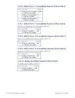
5.26
SSD Erase Control Register (Offset 0x6BF)
To trigger a hardware erase, software must write to a bit with a “1”, “0”, “1” pattern
on consecutive write cycles to this register. This is to protect against ‘accidental’
erase functions. The value read from this register represents the state of the output
and not the last value written.
Bits
Description
Default
7 to 1
SSD7:1 hardware erase:
0 = Hardware erase pin negated
0000000
b
0
SSD0 hardware erase:
1 = Hardware erase pin active
0 = Hardware erase pin negated
0
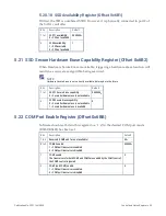
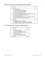
5.27
SSD Cache Flush Control Register (Offset 0x6C0)
The bits in this register directly control the Cache Flush pin of the corresponding
SSD device.
Bits
Description
Default
7 to 1
SSD7:1 cache flush:
0 = Cache flush pin negated
0000000
b
0
SSD0 cache flush:
1 = Cache flush pin active
0 = Cache flush pin negated
0
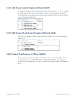
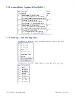
5.28
Scratch Pad Register 1 (Offset 0x6C6)
This is a generic read/write register available to software to validate FPGA access. It
is sticky when reset using BIT_HRESET or CPU_RESET_REQ_L. This register is
driven out in the processor POR_CFG word during Power-On/Reset. The default is
0x00.
Содержание PPC11A
Страница 1: ...Hardware Reference Manual PPC11A 6U VME Single Board Computer Edition 1 Publication No PPC11A HRM 1 ...
Страница 27: ...Publication No PPC11A HRM 1 Functional Description 27 Figure 4 2 Block Diagram T2081 ...
Страница 113: ...Publication No PPC11A HRM 1 Connectors 113 Figure 6 2 Rear Connector Position ...


