58 PPC11A 6U VME Single Board Computer
Publication No. PPC11A-HRM/1
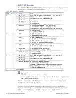
4.20.7 DIP Switches
Two NXP PCA9560 I
2
C EEPROM DIP Switch devices are used to configure certain
aspects of PPC11A operation as shown below:
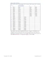
Table 4-29 PCA9560 Bit Meanings
Switch Register Bit Function
Details
1
0
0
XMC1 GA bit 2
For site 1 PMC deployments, program these to 5
D
(101
b
) to select 5V VIO.
Otherwise, VIO is 3.3V.
VIO is always set to 3.3V for combined XMCs/PMCs
1
XMC1 GA bit 1
2
XMC1 GA bit 0
3
SSD Write protect
0 = Write enable SSD
1 = Write protect SSD
4
RCW select
0 = Select RCW A (normally used to select 2 x 4-wire UART)
1 = Select RCW B (normally used to select 4 x 2-wire UART)
This bit has no effect if the RCW is loaded from the I
2
C EEPROM (see bit 5)
5
RCW source
0 = Load RCW from FPGA
1 = Load RCW from I
2
C EEPROM
1
1
0
GPIO4
0 = GPIO4 standard function
1 = Reserved for GPIO4 special function
1
GPIO5
0 = GPIO5 standard function
1 = Use GPIO5 as a duplicate Flash Password Unlock link input
2
GPIO6
0 = GPIO6 standard function
1 = Use GPIO6 as a duplicate Boot Alternate link input
3
GPIO7
0 = GPIO7 standard function
1 = Use GPIO7 as a duplicate Boot Recovery link input
4
Boot site swap
0 = Boot from Main boot image in NOR Flash
1 = Boot from Alternate boot image in NOR Flash
5
NVRAM write protect
0 = Write-enable NVRAM
1 = Write-protect NVRAM
2
0
0
XMC2 GA bit 2
For site 2 PMC deployments, program these to 5
D
(101
b
) to select 5V VIO.
Otherwise, VIO is 3.3V.
VIO is always set to 3.3V for combined XMCs/PMCs
1
XMC2 GA bit 1
2
XMC2 GA bit 0
3
Outbound VMEbus path 0 = Disable second (outbound) VMEbus path
1 = Enable second (outbound) VMEbus path
This is used to enable the two-path (inbound/outbound) VME architecture.
It may also be useful during configuration of the two-path architecture.
This is not currently implemented
2
1
Not implemented
NOTES
The PPC11A must be reset for any updates to take effect.
PMC1 and PMC2 5V VIO Selection Links (P15 Pins 13 to 16)
override DIP Switch 1 register 0 bits 0 to 2
and DIP Switch 2 register 0 bits 0 to 2.
The devices are write-enabled only when a jumper is fitted on the
Write Enable link (P15 pins 9 and 10)
The DIP switch settings are shown in the EEPROM DIP Switch Configuration
for Switch 1 Register 0,
for Switch 2 Register 0 [Switch 2 Register 1 is not implemented).
Содержание PPC11A
Страница 1: ...Hardware Reference Manual PPC11A 6U VME Single Board Computer Edition 1 Publication No PPC11A HRM 1 ...
Страница 27: ...Publication No PPC11A HRM 1 Functional Description 27 Figure 4 2 Block Diagram T2081 ...
Страница 113: ...Publication No PPC11A HRM 1 Connectors 113 Figure 6 2 Rear Connector Position ...


