


118 PPC11A 6U VME Single Board Computer
Publication No. PPC11A-HRM/1
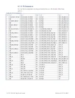
Signal
Description
GAP~
Geographical addressing parity bit input. The sum of all GA bits, including the parity bit, should be an odd number
GND
Signal Ground
NC
No connection
NVM_WE~
Replicates the effect of the
(signals are ORed in the FPGA)
PMC1_[01:64]
Rear I/O signals from PMC site 1 (J14 connector). Signal names reflect the pin numbers of this connector
PMC2_[01:64]
Rear I/O signals from PMC site 2 (J24 connector). Signal names reflect the pin numbers of this connector
SATA_RXyN/P,
SATA_TXyN/P
SATA channel y (y = 0 or 1) Receive input and Transmit output differential pairs
SMBUS_CLK,
SMBUS_DATA
System Management bus clock and data. Connected to the BMM via an I
2
C buffer. Allows access to certain on-board
resources from an external I
2
C master
SYSRESET~
System-wide reset. Driven low by the PPC11A if configured as System Controller
TDO, TDI, TCK, TMS,
TRST~
JTAG interface
USBn_N/P
Universal Serial Bus n (n = 1 or 2) differential pairs
USB_PWR
Universal Serial Bus switched power output (5V)
VGA_RED,
VGA_GREEN,
VGA_BLUE,
VGA_HSYNC,
VGA_VSYNC
VGA red,
green,
blue,
horizontal synchronization,
vertical synchronization
XMC1_x[01:19]
Rear I/O signals from XMC site 1 (J16 connector). Signal names reflect the pin numbers of this connector
+12V
VME +12V auxiliary power input. Connected to the PMC/XMC sites, otherwise unused by the PPC11A
-12V
VME -12V auxiliary power input. Connected to the PMC/XMC sites, otherwise unused by the PPC11A
+5V
VME +5V power input
+5VSTDBY
Battery supply. Can be used to power the RTC on the PPC11A (requires up to 1µA)
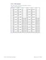
Figure 6-3 RS422/485 Signal Waveforms
Содержание PPC11A
Страница 1: ...Hardware Reference Manual PPC11A 6U VME Single Board Computer Edition 1 Publication No PPC11A HRM 1 ...
Страница 27: ...Publication No PPC11A HRM 1 Functional Description 27 Figure 4 2 Block Diagram T2081 ...
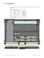
Страница 113: ...Publication No PPC11A HRM 1 Connectors 113 Figure 6 2 Rear Connector Position ...


