


ZC706 Evaluation Board User Guide
18
UG954 (v1.5) September 10, 2015
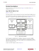
Feature Descriptions
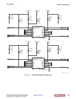
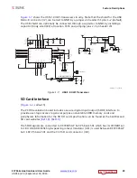
DDR3 SODIMM Memory (PL)
[
, callout 2]
The memory module at J1 is a 1 GB DDR3 small outline dual-inline memory module
(SODIMM). It provides volatile synchronous dynamic random access memory (SDRAM) for
storing user code and data.
• Part number: MT8JTF12864HZ-1G6G1 (Micron Technology)
• Supply voltage: 1.5V
• Datapath width: 64 bits
• Data rate: Up to 1,600 MT/s
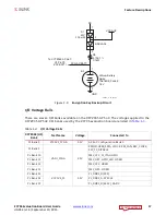
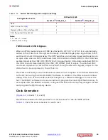
The DDR3 interface is implemented across the PL-side I/O banks. Bank 33 and bank 35 have
a dedicated DCI VRP/N resistor connection. An external 0.75V reference VTTREF_SODIMM is
provided for data interface banks. Any interface connected to these banks that requires the
VTTREF voltage must use this FPGA voltage reference. The connections between the DDR3
memory and the AP SoC are listed in
.
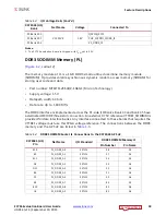
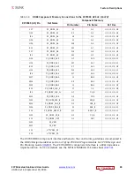
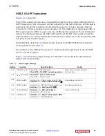
PS Bank 500
VCCP1V8
1.8V
QSPI0,QSPI1
PS Bank 501
PHY_IF,SDIO_IF,USB_IF
PS Bank 502
PS_DDR3_IF
Notes:
1. The ZC706 evaluation board is shipped with V
ADJ
set to 2.5V.
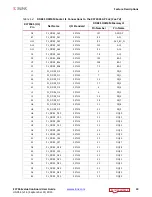
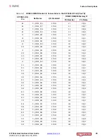
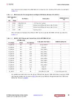
Table 1-4:
DDR3 SODIMM Socket J1 Connections to the XC7Z045 AP SoC
XC7Z045 (U1)
Pin
Net Name
I/O Standard
DDR3 SODIMM Memory J1
Pin Number
Pin Name
E10
PL_DDR3_A0
SSTL15
98
A0
B9
PL_DDR3_A1
SSTL15
97
A1
E11
PL_DDR3_A2
SSTL15
96
A2
A9
PL_DDR3_A3
SSTL15
95
A3
D11
PL_DDR3_A4
SSTL15
92
A4
B6
PL_DDR3_A5
SSTL15
91
A5
F9
PL_DDR3_A6
SSTL15
90
A6
E8
PL_DDR3_A7
SSTL15
86
A7
B10
PL_DDR3_A8
SSTL15
89
A8
J8
PL_DDR3_A9
SSTL15
85
A9
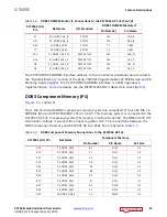
Table 1-3:
I/O Voltage Rails
(Cont’d)
XC7Z045 (U1)
Bank
Net Name
Voltage
Connected To