


ZC706 Evaluation Board User Guide
16
UG954 (v1.5) September 10, 2015
Feature Descriptions
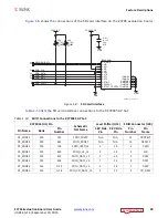
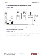
• PL Configuration: USB JTAG configuration port (Digilent module U30)
• PL Configuration: Platform cable header J3 and flying lead header J62 JTAG
configuration ports
TIP:
Designs using serial configuration based on Quad-SPI flash memory can take advantage of
low-cost commodity SPI flash memory.
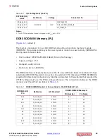
The JTAG configuration option is selected by setting SW11 (PS) as shown in
SW4 (PL) as described in
Programmable Logic JTAG Programming Options, page 31
. SW11
is callout
.
For more information about Zynq-7000 AP SoC configuration settings, see
Zynq-7000 All
Programmable SoC Technical Reference Manual (
)
.
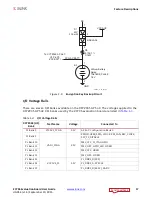
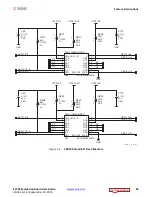
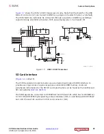
Encryption Key Backup Circuit
The XC7Z045 AP SoC U1 implements bitstream encryption key technology. The ZC706
board provides the encryption key backup battery circuit shown in
. The Seiko
TS518FE rechargeable 1.5V lithium button-type battery B2 is soldered to the board with the
positive output connected to the XC7Z045 AP SoC U1 VCCBATT pin P9. The battery supply
current IBATT specification is 150 nA max when board power is off. B2 is charged from the
VCCAUX 1.8V rail through a series diode with a typical forward voltage drop of 0.38V and
4.7 K
Ω
current limit resistor. The nominal charging voltage is 1.42V.
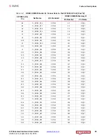
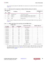
Table 1-2:
Switch SW11 Configuration Option Settings
Boot Mode
SW11.1
SW11.2
SW11.3
SW11.4
SW11.5
JTAG mode
0
0
0
0
0
Independent JTAG mode
1
0
0
0
0
QSPI mode
0
0
0
1
0
SD mode
0
0
1
1
0
MIO configuration pin
MIO2
MIO3
MIO4
MIO5
MIO6
Notes:
1. Default switch setting


