
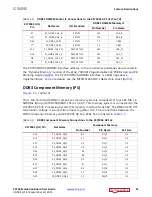

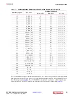


ZC706 Evaluation Board User Guide
31
UG954 (v1.5) September 10, 2015
Feature Descriptions
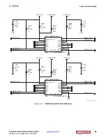
Programmable Logic JTAG Programming Options
[
, callout 6]
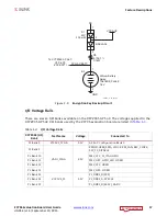
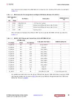
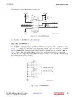
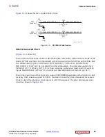
The ZC706 evaluation board JTAG chain is shown in
.
Programmable Logic JTAG Select Switch
[
, callout 35]
The PL JTAG chain can be programmed by three different methods made available through
a 3-to-1 analog switch (U45, U46, and U47) controlled by a 2-position DIP switch at SW4.
shows the JTAG analog switches and DIP switch SW4.
X-Ref Target - Figure 1-9
Figure 1-9:
JTAG Chain Block Diagram
UG954_c1_09_041113
3.3V
3.3V
FMC HPC
Connector
TDI TDO
J37
U1
Zynq-7000
XC7Z045
AP SoC
TDI
TDO
SN74AVC2T245
and
SN74LV541APWR
Buffers
TDI
TDO
U10
FMC LPC
Connector
TDI TDO
J5
SPST Bus Switch
U32
N.C.
N.C.
SPST Bus Switch
U31
JTAG
Module
TDO
TDI
U30
JTAG
Header
TDO
TDI
J3
JTAG
Header
TDO
TDI
J62
3:1
Analog
Switch
U45
U46
U47
SW4
1
2
ON


